Group III nitride compound semiconductor device and method for producing the same

a technology of nitride and compound semiconductors, applied in the direction of semiconductor lasers, solid-state devices, semiconductor lasers, etc., can solve problems such as cracking, and achieve the effect of efficiently providing to the substrate surfa

Inactive Publication Date: 2006-01-03
TOYODA GOSEI CO LTD
View PDF39 Cites 106 Cited by
  • Summary
  • Abstract
  • Description
  • Claims
  • Application Information

AI Technical Summary

Benefits of technology

[0028]When the second environment division is constituted by a separation layer of silicon oxide, or the like, the exposed substrate surface in the first environment division is in a so-called “valley floor” state by the presence of the separation layer. To form group III nitride compound semiconductor layers on such a substrate surface efficiently by an MOCVD method, at least a carrier

Problems solved by technology

When things come to the worst, cracking may occur.
The problem that stress due to the difference between the thermal expansion coefficients is caused in the group III nitride compound semicond

Method used


Image

  • Group III nitride compound semiconductor device and method for producing the same
  • Group III nitride compound semiconductor device and method for producing the same
  • Group III nitride compound semiconductor device and method for producing the same

Examples


first embodiment

(First Embodiment)

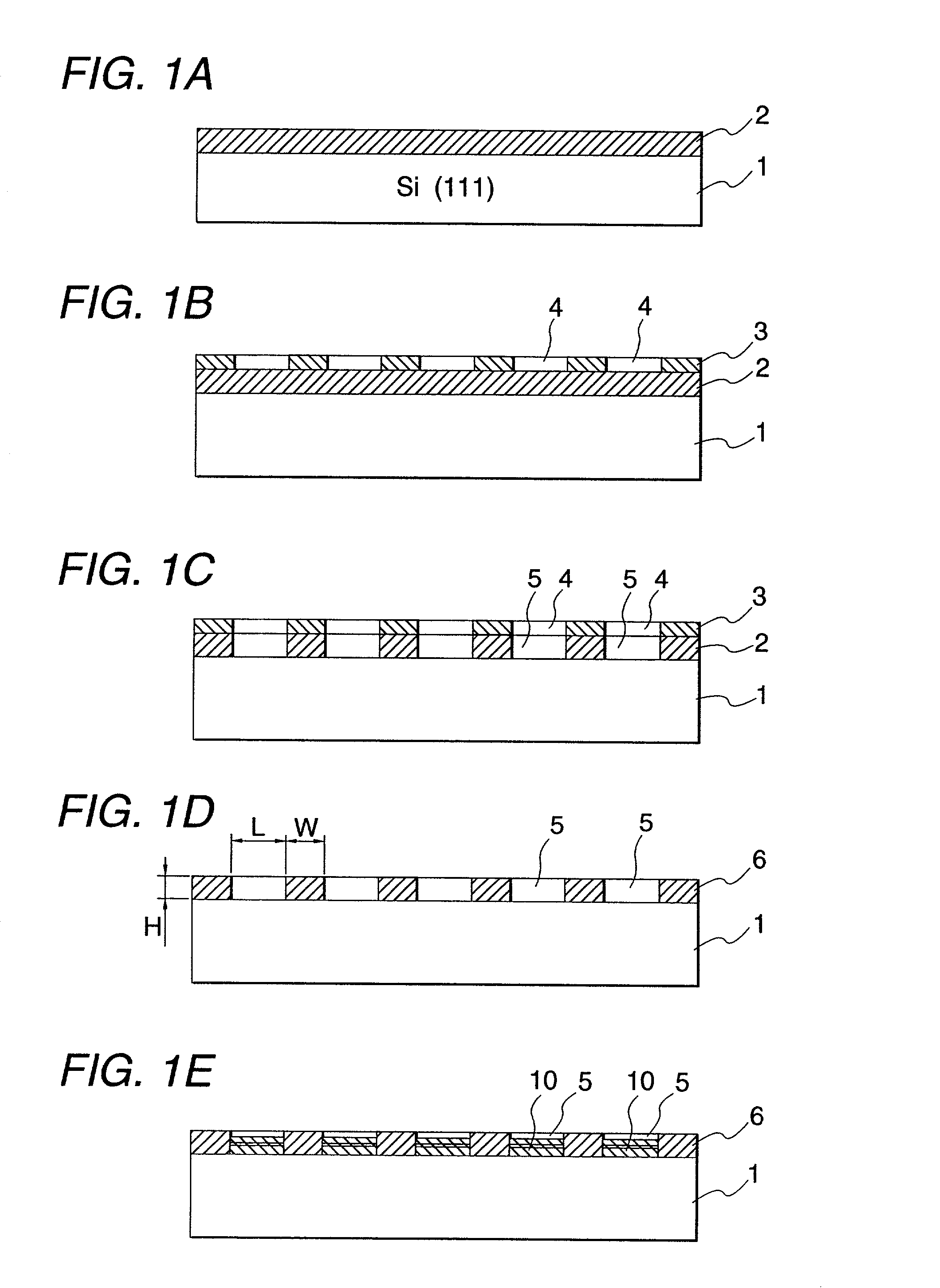
[0041]FIG. 1 is a process view showing the outline of a producing method according to an embodiment.

[0042]In this embodiment, a silicon substrate 1 (diameter: 2 inches) is prepared and a silicon oxide layer 2 for constituting a second environment division is formed on a (111) face of the substrate 1 by a CVD method (see FIG. 1A). The thickness of the silicon oxide layer 2 is set to be about 5.5 μm.

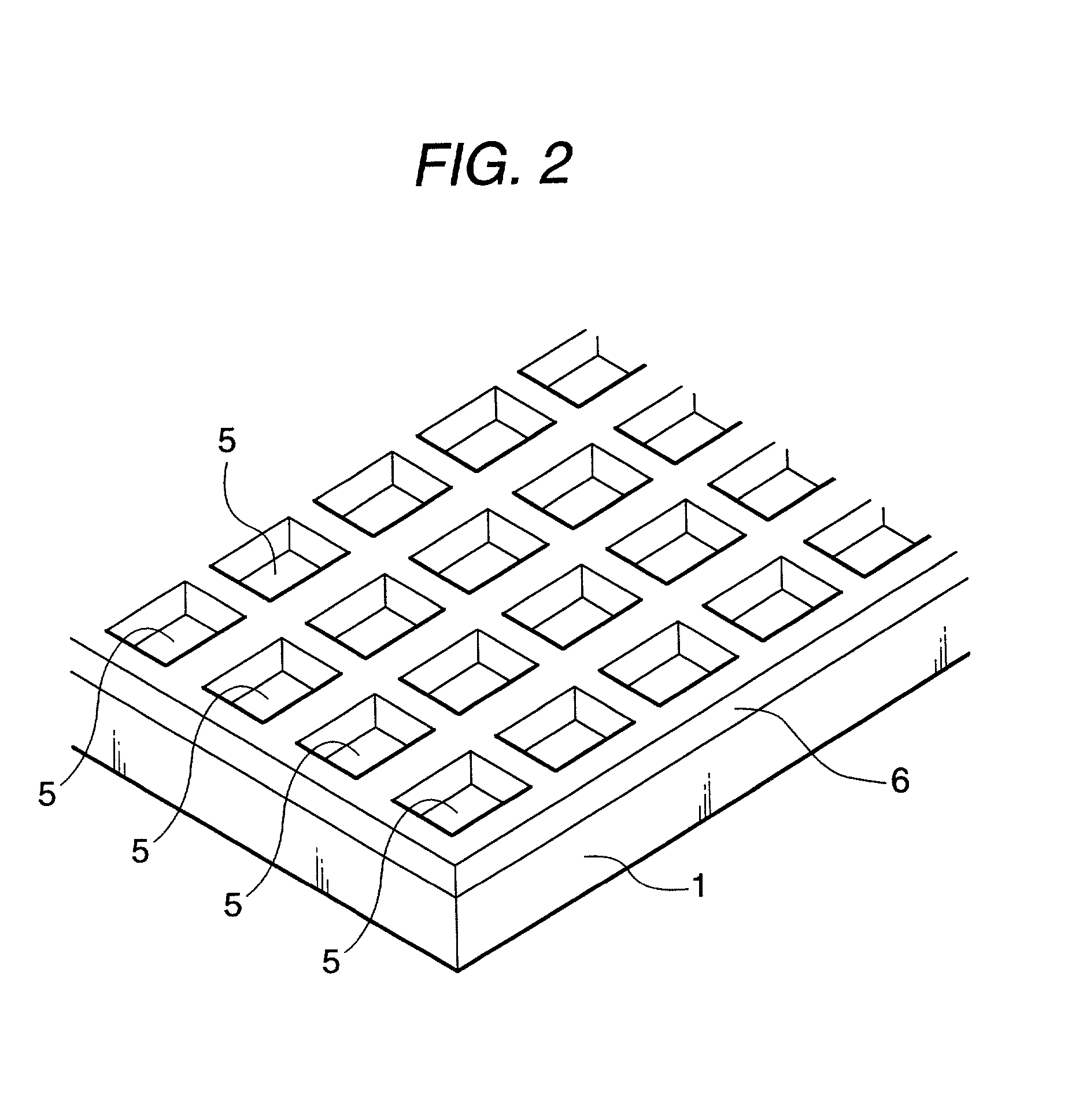
[0043]Then, as shown in FIG. 1B, a mask layer 3 is formed as a pattern on the silicon oxide layer 2, and the silicon oxide layer 2 is subjected to wet etching through opening portions 4 of the mask layer 3. Consequently, as shown in FIG. 1C, opening portions 5 for constituting first environment divisions are formed in the silicon oxide layer 2, so that the silicon substrate 1 is exposed in the opening portions 5.

[0044]Then, as shown in FIG. 1D, the mask layer 3 is removed. Consequently, the silicon oxide layer having the opening portions 5 form a separation layer 6.

[0045]...

second embodiment

(Second Embodiment)

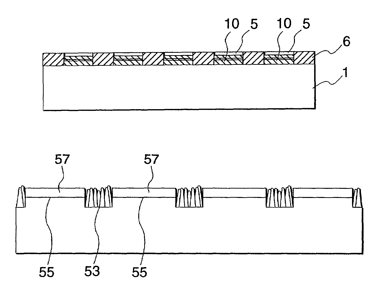
[0077]A producing method according to another embodiment of this invention will be described.

[0078]As shown in FIG. 9A, for example, grooves 53 with a width W of about 25 μm and a depth H of from about 5 to about 10 μm at intervals L of 350 μm are formed in x and y directions, in a surface of a silicon substrate 51 by using half-cutting by means of a dicing blade. Thus, square portions (first environment divisions) 55 with each side about 325 μm long are formed so as to be surrounded by the 25 μm-wide grooves 53 in four directions. Each of the square portions 55 has a shape and size corresponding to the shape of a semiconductor device.

[0079]Incidentally, bottom and side faces of the grooves 53 are roughened by half-cutting by means of a dicing blade.

[0080]When a group III nitride compound semiconductor is grown on the substrate 51 provided with such grooves 53, a single crystal group III nitride compound semiconductor layer 57 of good crystallinity is grown on eac...


PUM


Abstract

A group III nitride compound semiconductor device is produced according to the following manner. A separation layer made of a material which prevents group III nitride compound semiconductors from being grown thereon is formed on a substrate. Group III nitride compound semiconductors is grown on a surface of the substrate uncovered with the separation layer while keeping the uncovered substrate surface separated by the separation layer.

Description

[0001]This is a divisional application of U.S. application Ser. No. 09 / 522,833, filed on Mar. 10, 2000 now U.S. Pat. No. 6,342,404, the contents of which are incorporated herein by reference.BACKGROUND OF THE INVENTION[0002]1. Field of the Invention[0003]The present invention relates to a group III nitride compound semiconductor device and a method for producing the same.[0004]The present application is based on Japanese Patent Application No. Hei. 11-92948, which is incorporated herein by reference.[0005]2. Description of the Related Art[0006]A group III nitride compound semiconductor device is formed from group III nitride compound semiconductors grown on a substrate such as a sapphire substrate by a method such as an MOCVD method. On the other hand, a technique using a silicon or silicon carbide substrate inexpensive and itself electrically conductive for growing group III nitride compound semiconductor layers thereon has been examined.[0007]In the case of a silicon substrate, ho...

Claims


Application Information

Patent Timeline
IPC IPC(8): H01L31/0256H01L21/20H01L21/205H01L31/10H01L33/00H01L33/06H01L33/12H01L33/16H01L33/32H01L33/34H01S5/00H01S5/323H01S5/343
CPCH01L21/02381H01L21/0242H01L33/007H01L21/0254H01L21/02639H01L21/02458
Inventor SHIBATA, NAOKIITO, JUNCHIYO, TOSHIAKIASAMI, SHIZUYOWATANABE, HIROSHIASAMI, SHINYA
Owner TOYODA GOSEI CO LTD
Why Eureka
Try Eureka