

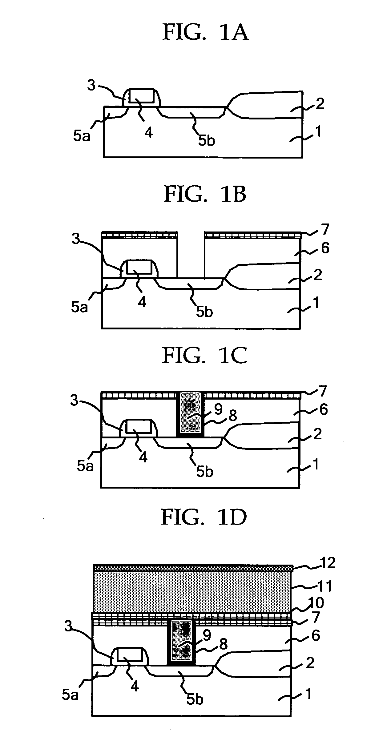
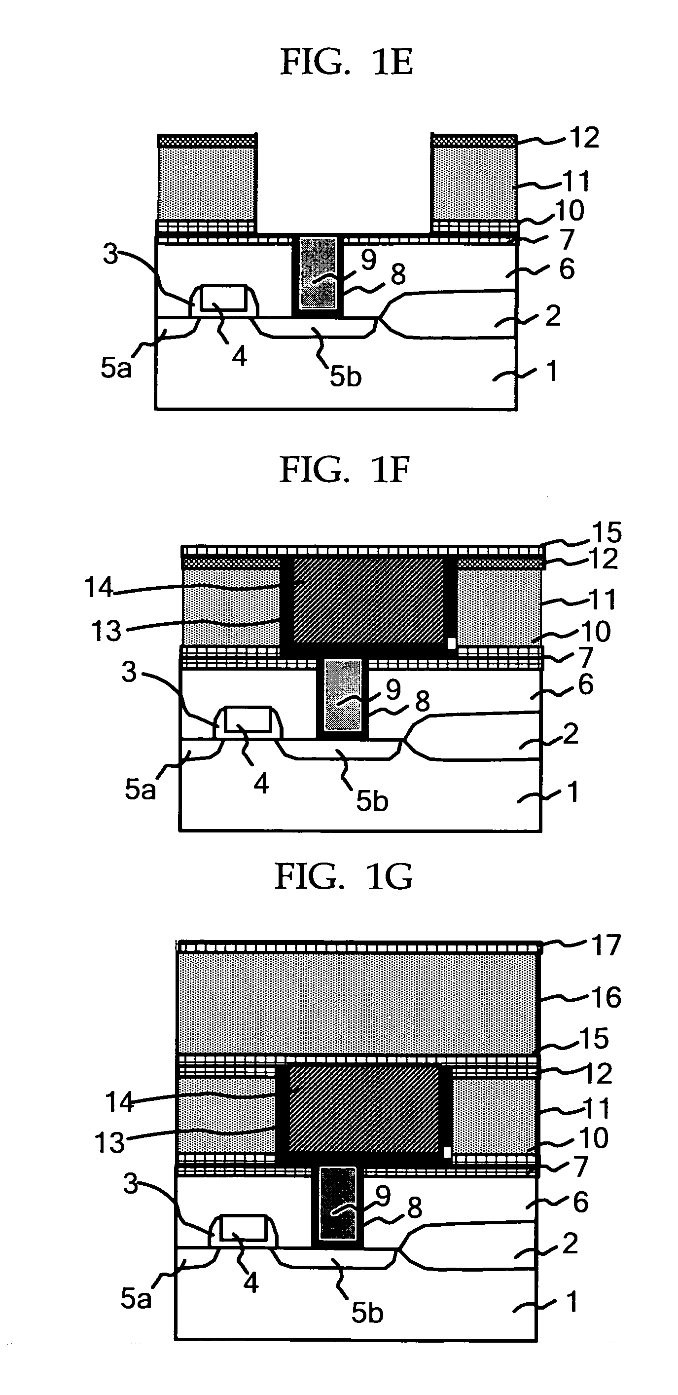
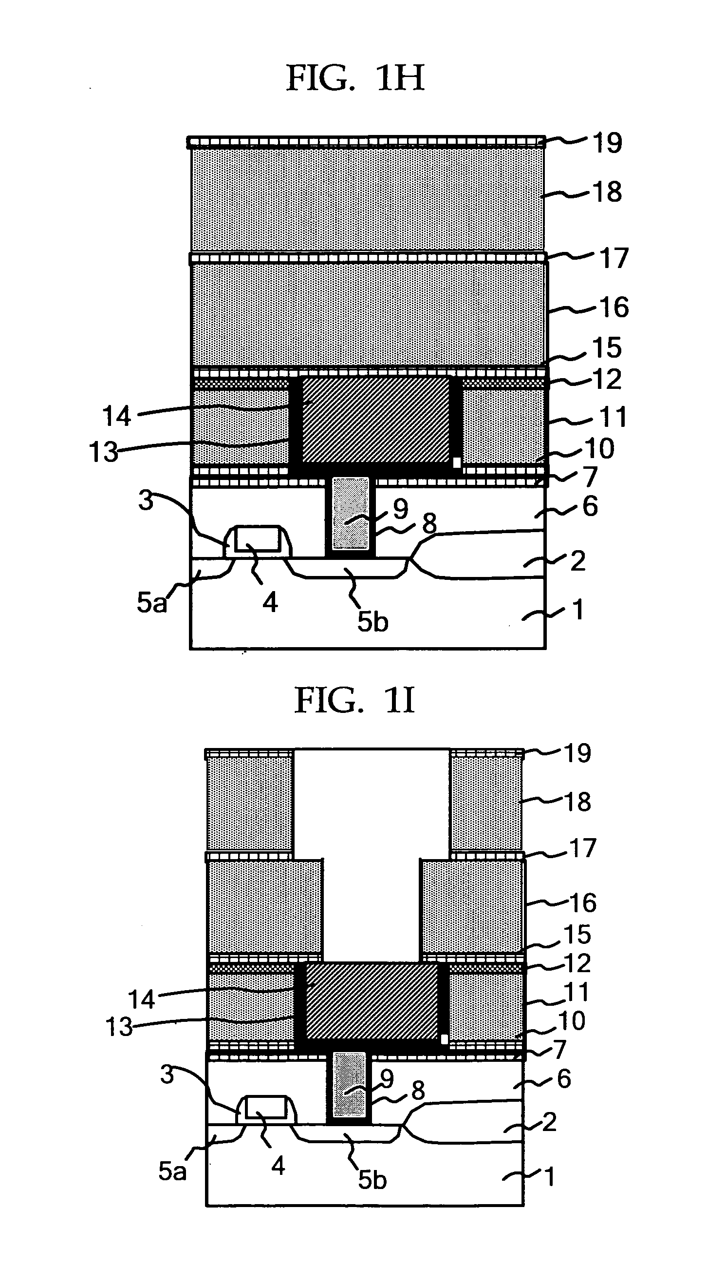
Silica film forming material, silica film and method of manufacturing the same, multilayer wiring structure and method of manufacturing the same, and semiconductor device and method of manufacturing the same
a technology of silica film and silica film, which is applied in the direction of semiconductor devices, transportation and packaging, coatings, etc., can solve the problems of further increase of wiring resistance (t), reduced capacity (c) and wiring delay, and achieves reduced parasitic capacity, improved signal transmission speed, and higher response speed
- Summary
- Abstract
- Description
- Claims
- Application Information
AI Technical Summary
Benefits of technology
Problems solved by technology
Method used
Image

Examples
examples
[1054] Examples of the present invention will be described below, however, the present invention is not limited to the following examples.
examples 1 to 27
--Preparation of Silica Film Forming Material--
[1055] Into a 4-mouth flask, 1,2-bis(dimethylethoxysilyl)ethane (1,2-DMESE) and 1,4-bis (dimethylethoxysilyl) benzene (1,4-DMESB), which are the silicon compounds expressed by the structural formula (3); tetraethoxysilane (TEOS) which is the silicon compound expressed by the structural formula (4); and methyltriethoxysilane (MTEOS) and phenyltriethoxysilane (PTEOS), which are the silicon compounds expressed by the structural formula (5); 500 ppm nitric acid water; and propylene glycolmonomethylether as the organic solvent were poured in the amounts shown in Tables 1 to 3, respectively, and hydrolysis condensation polymerization reaction was performed over a 2 hour period at 50° C., thereby preparing the silica film forming materials.
--Manufacturing Silica Film--
[1056] Each silica film forming material thus obtained was coated onto the silicon wafer by way of spin coating at 1,500 rpm of rotation speed for 1 minute so as to have a t...
examples 28 to 54
--Preparation of Silica Film Forming Material--
[1075] Into a 4-mouth flask, 1,2-bis (dimethylchlorosilyl) ethane (1,2-DMCSE) and 1,4-bis (dimethylchlorosilyl) benzene (1,4-DMCSB), which are the silicon compounds expressed by the structural formula (10); etrachlorosillan (TCS) which is the silicon compound expressed by the structural formula (11); methyltrichlorosillan (MTCS) and phenyltrichlorosillan (PTCS), which are the silicon compounds expressed by the structural formula (12); 500 ppm nitric acid water; and propylene glycolmonomethylether as the organic solvent were poured in the amounts shown in Tables 5 to 7, respectively, and hydrolysis condensation polymerization reaction was performed over a 2 hour period at 50° C., thereby preparing the silica film forming materials.
[1076] The silica films of Examples 28 to 54 were manufactured by using the silica film forming materials thus obtained in the same manner as in Example 1. Further, the characteristics of the respective sili...
PUM
| Property | Measurement | Unit |
|---|---|---|
| pH | aaaaa | aaaaa |
| temperature | aaaaa | aaaaa |
| dielectric constant | aaaaa | aaaaa |
Abstract
Description
Claims
Application Information