Semiconductor device and manufacturing method thereof

a semiconductor device and manufacturing method technology, applied in the direction of semiconductor devices, semiconductor/solid-state device details, electrical apparatus, etc., can solve the problems of disconnection of the wiring, and separation between the wirings, so as to increase the parasitic capacity between the wirings, high integration of the semiconductor device, and high density of the wiring

Inactive Publication Date: 2005-10-25
TRECENTI TECHNOLOGIES INC
View PDF6 Cites 0 Cited by
  • Summary
  • Abstract
  • Description
  • Claims
  • Application Information

AI Technical Summary

Benefits of technology

[0005]With high integration of the semiconductor device in recent years, high density of wirings by their micro-fabrication has been demanded. However, parasitic capacity between the wirings has been increased depending on the high density of the wirings, which leads to delay in sending electric signals. Thus, it is desirable to adopt a material having as low a dielectric constant as possible as the interlayer insulation film between the wiring layers to reduce such parasitic capacity.

Problems solved by technology

However, parasitic capacity between the wirings has been increased depending on the high density of the wirings, which leads to delay in sending electric signals.
By application of such a pulling stress, there arises the problem of disconnection of the wiring, separation between the wiring and the insulation film, and the like.
The problem has a significant tendency to occur, in a semiconductor device having large integrated value in thickness of the low-dielectric-constant insulation film, particularly, in a step of manufacturing a semiconductor device with many wiring layers.
Due to this stress, there is the problem that the lower-dielectric-constant insulation films are separated from one another between the low-dielectric-constant insulation films to be laminated, and there is the problem that disconnection by stress migration occurs between the wiring layers.

Method used


Image

  • Semiconductor device and manufacturing method thereof
  • Semiconductor device and manufacturing method thereof
  • Semiconductor device and manufacturing method thereof

Examples


first embodiment

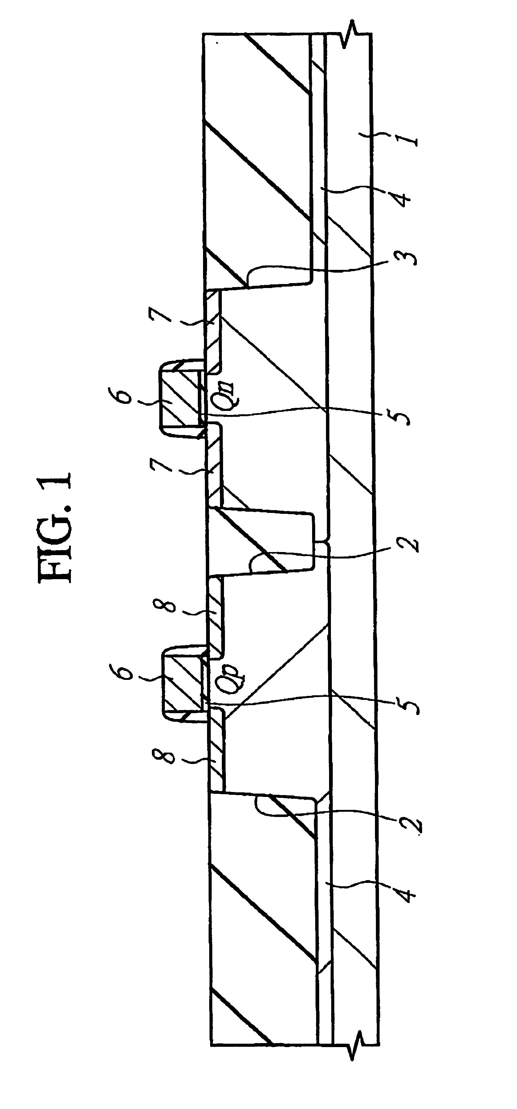
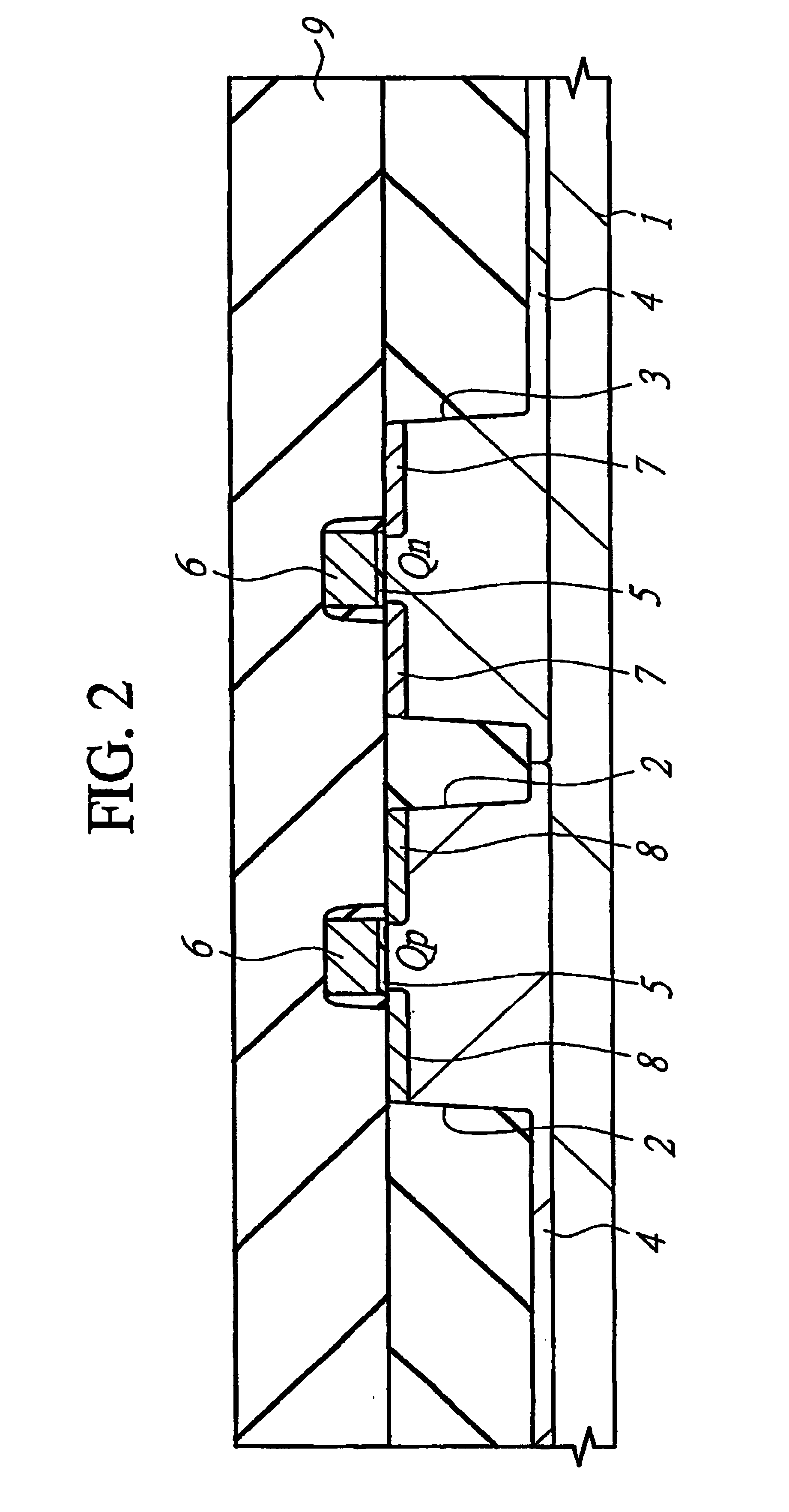
[0042](First Embodiment)

[0043]A semiconductor device according to this first embodiment has a CMISFET (Complementary MISFET). The manufacturing process of a semiconductor device according to the first embodiment will be described with reference to FIGS. 1 to 16.

[0044]As shown in FIG. 1, a semiconductor substrate 1 made of monocrystal silicone having a specific resistance of approximately 10 Ωcm is thermally treated at approximately 850° C., and a thin silicone oxide film (pad oxide film) having a thickness of 10 nm is formed on its main surface (device formation surface). Next, a silicone nitride film with a thickness of approximately 120 nm is deposited on this silicone oxide film by a CVD (Chemical Vapor Deposition) method and, thereafter, the silicone nitride film and the silicone oxide film in a device separation region are removed by dry etching using a photoresist film as a mask. The silicone oxide film is formed in order to relax a stress applied to the substrate at the time ...

second embodiment

[0076](Second Embodiment)

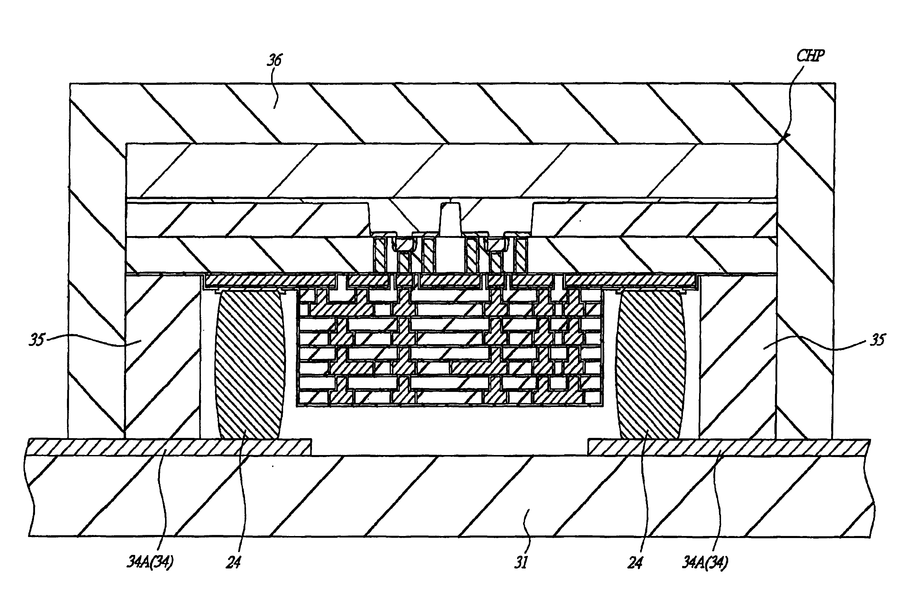
[0077]FIG. 18 is a sectional view showing a principal portion of a semiconductor device in a manufacturing process according to a second embodiment. In a second embodiment as shown in FIG. 18, the semiconductor chip CHP is packaged using the insulation tape 31 from which the resin member 35 (see FIGS. 15 to 17) described in the first embodiment is omitted. The resin 36 sealing the rear and side surfaces of the semiconductor chip CHP has viscosity in an non-solidified condition, and so if a plurality of bump electrodes 24 adjacent thereto are formed at an interval smaller than a predetermined one, the resin 36 cannot flow into the main surface side of the semiconductor chip CHP through a gap between the adjacent bump electrodes 24. That is, it is possible to provide the bump electrodes 24 with the same function as that of the resin member 35 shown in FIG. 1.

[0078]Also, as shown in FIG. 19, even if the insulation tape 31 from which the resin member 35 is omitt...


PUM


Abstract

In a semiconductor device manufacturing process using a low-dielectric-constant insulation film as an interlayer insulation film, a stress exerted on wiring layers and interlayer insulation films is reduced. In a semiconductor device in which a plurality of buried wiring layers are formed in the interlayer insulation films each formed of a low-dielectric-constant insulation film lower in mechanical strength than a silicone oxide film formed by, for example, a CVD method, a first layer of wiring, on a lower layer of which a low-dielectric-constant insulation film is not disposed, serves as a bonding pad, and bump electrodes are formed on the wiring so as to become higher than a position where the uppermost buried wiring is formed.

Description

CROSS-REFERENCE TO RELATED APPLICATION[0001]The present application claims priority from Japanese patent application No. JP 2003-153613 filed on May 30, 2003, the content of which is hereby incorporated by reference into this application.BACKGROUND OF THE INVENTION[0002]The present invention relates to a semiconductor device and a manufacturing technique thereof and, particularly, to a technique effectively applied to manufacture of a semiconductor device having an interlayer insulation film with low dielectric constant between wiring layers.[0003]For example, in a semiconductor device including an organic insulation film with low dielectric constant and with low hardness and low elasticity as an interlayer insulation film between wiring layers, there is a technique in which, since a dummy wiring and a connection hole are provided under a bonding pad, destruction of the interlayer insulation film and boundary separation between the wiring layers and the interlayer insulation film ar...

Claims


Application Information

Patent Timeline
Patent Type & Authority Patents(United States)
IPC IPC(8): H01L23/48H01L23/522H01L23/52H01L23/485H01L23/532H01L21/3205H01L21/60
CPCH01L23/522H01L24/13H01L24/02H01L24/10H01L23/53238H01L2924/1306H01L2924/01033H01L2224/0401H01L2224/13099H01L2924/01004H01L2924/01005H01L2924/01006H01L2924/01013H01L2924/01014H01L2924/01015H01L2924/01022H01L2924/01029H01L2924/0105H01L2924/01057H01L2924/01073H01L2924/01074H01L2924/01078H01L2924/01079H01L2924/01082H01L2924/014H01L2924/04941H01L2924/04953H01L2924/12044H01L2924/30105H01L2924/00H01L2224/13H01L2224/14155H01L24/14H01L24/05H01L24/16H01L2224/05569H01L2224/13024
Inventor TOKUNAGA, KENJI
Owner TRECENTI TECHNOLOGIES INC
Why Eureka
Try Eureka