Method of producing a carbon nanotube and a carbon nanotube structure
a carbon nanotube and carbon nanotube technology, applied in the field of carbon nanotube and carbon nanotube structure, can solve the problems of difficult preparation of structures having desirable properties, and achieve the effects of eliminating various problems, superior production stability, and high yield
- Summary
- Abstract
- Description
- Claims
- Application Information
AI Technical Summary
Benefits of technology
Problems solved by technology
Method used
Image
Examples
first embodiment
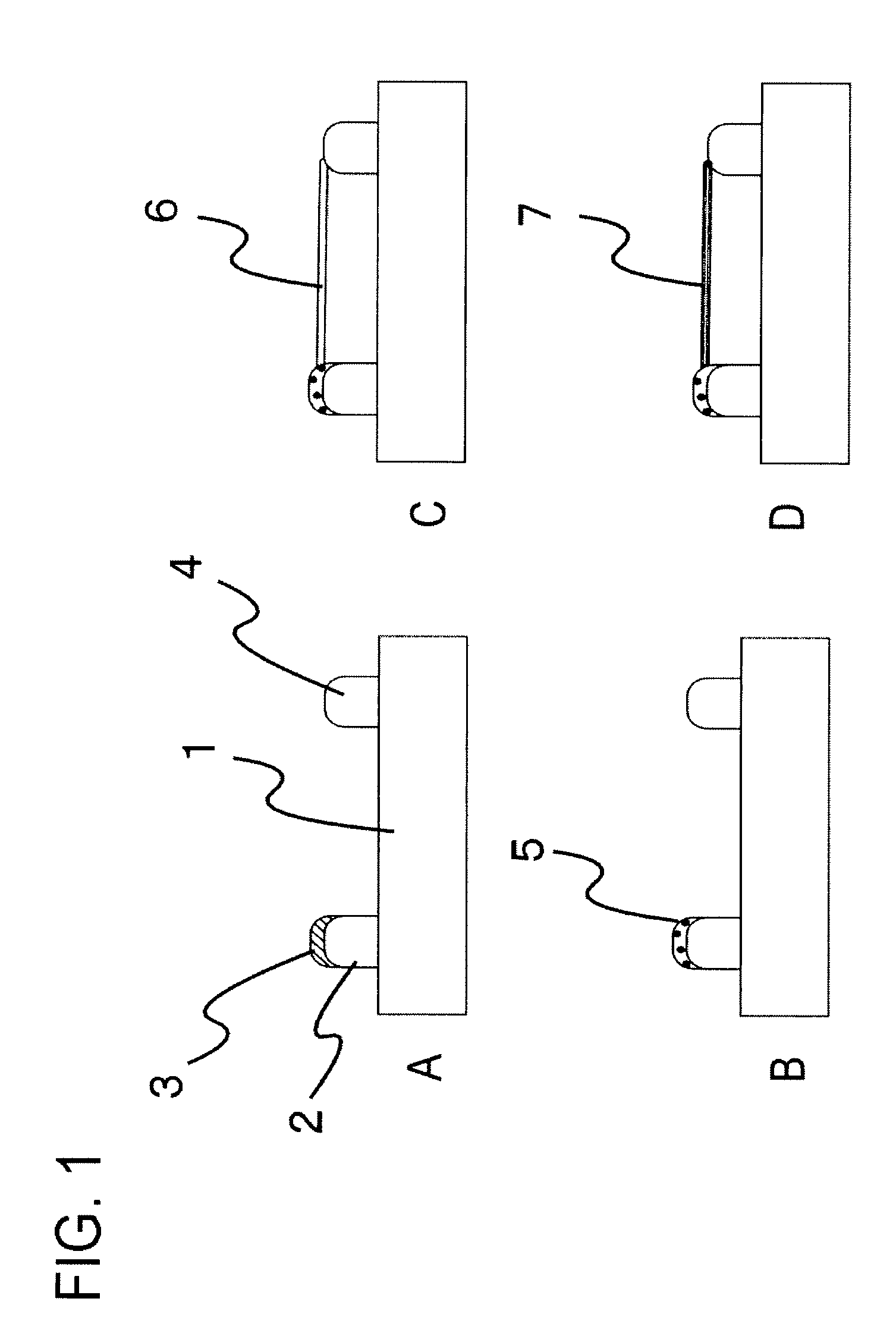
[0049] The method of producing a carbon nanotube according to this embodiment will be described below.
[0050] First, a metal fine particle to be a catalyst is placed on a substrate forming a carbon nanotube. The material for the substrate is not particularly limited, and may be selected from various materials such as silicon, according to applications.
[0051] The catalyst metal is selected from metals higher in the activity of graphitizing reaction such as Fe, Ni, Co, Cr, and Mo. Alternatively, an alloy containing at least one of these metals may also be used. For example, even an alloy of the metal above and a metal having no activity of graphitizing reaction such as FePt or NiCu alloy is occasionally effective, because such an alloy sometimes has an activity higher than the constituent single metal such as Fe or Ni. In addition, an alloy containing various metals often has an effect of lowering melting point, and is thus effective.
[0052] The metal fine particle is commonly prepar...
second embodiment
[0086] In the present embodiment, metal catalyst fine particles are prepared according to a method of patterning by a lithographic process. Therefore, it relates to a production method favorable for mass production of carbon nanotubes and the devices containing that.
[0087] First, a window of positive resist is formed on the terminal position for placing a carbon nanotube of a substrate for preparation of carbon nanotube. For example, it is possible to form a window of 10 nm in diameter easily in a process forming a three-layer resist, for example, of PMMA / Ge / PMMA.
[0088] In addition, it is possible to form an iron thin film only at a desirable position by vapor depositing a catalyst metal to a thickness of approximately 1 nm on the entire substrate surface and removing the undesirable regions by lift off and to form metal catalyst fine particles of 1 to 5 nm in diameter by heating the substrate further to approximately 600° C.
[0089] It is also possible to coat metal fine particles...
third embodiment
[0093] The present embodiment will be described in detail with reference to FIG. 4.
[0094] The embodiment relates to a method for preparation of nanotube amorphous carbon in which patterning is performed by a lithographic process, therefore, indicates a production method suitable for mass production of carbon nanotubes and the devices containing that.
[0095] First, a substrate 21 having a pattern made with catalyst metal fine particles 22 of approximately 8 nm in diameter is prepared by the method described in the first or second embodiment. The substrate 21 used is a plate of silicon oxide (FIG. 4A).
[0096] An organic high-resolution negative resist film of calixarene or polymethylstyrene is then prepared. Then, a one-dimensional structure 23 covering a fine particle 22 is formed by exposing and developing the one-dimensional region. In the embodiment, an amorphous carbon wire having a height of 5 nm, a width of 7 nm, and a length of 200 nm is formed by electron beam exposure by us...
PUM
| Property | Measurement | Unit |
|---|---|---|
| diameter | aaaaa | aaaaa |
| diameter | aaaaa | aaaaa |
| width | aaaaa | aaaaa |
Abstract
Description
Claims
Application Information


