Packaging Structure of AC light-emitting diodes

a technology of ac light-emitting diodes and packaging structures, which is applied in the direction of basic electric elements, electrical apparatus, and semiconductor devices, etc., can solve the problems of increased power consumption, reduced reliability of products, and increased power consumption, and achieves the effect of increasing power consumption

Inactive Publication Date: 2011-04-21
FORWARD ELECTRONICS CO LTD
View PDF2 Cites 26 Cited by
  • Summary
  • Abstract
  • Description
  • Claims
  • Application Information

AI Technical Summary

Benefits of technology

[0009]The object of the present invention is to provide a packaging structure of AC LEDs, which can pass the impact test of high voltage, and can prevent the problem of current-leakage and increased power consumption.

Problems solved by technology

Further, when the amount of the conductive silver paste 13 is too much to adhere on the circuit layer of the LED die 11, it may cause the problem of current-leakage and increased power consumption, and the reliability of the products may be decreased.
Hence, the bonding between the LED die and the heat dissipating base (not shown in the figure) of the carrier is not good enough.
In addition, the Ag particles with big diameters may cause holes to be formed in the conductive silver paste.
When the product is baked at high temperature, the conductive silver paste may become cracked, and the heat dissipating efficiency may be decreased.
However, when the aforementioned packaging structure of the LED is applied on an AC LED, the insulating effect of the conductive silver paste is not good enough.

Method used


Image

  • Packaging Structure of AC light-emitting diodes
  • Packaging Structure of AC light-emitting diodes
  • Packaging Structure of AC light-emitting diodes

Examples


Embodiment Construction

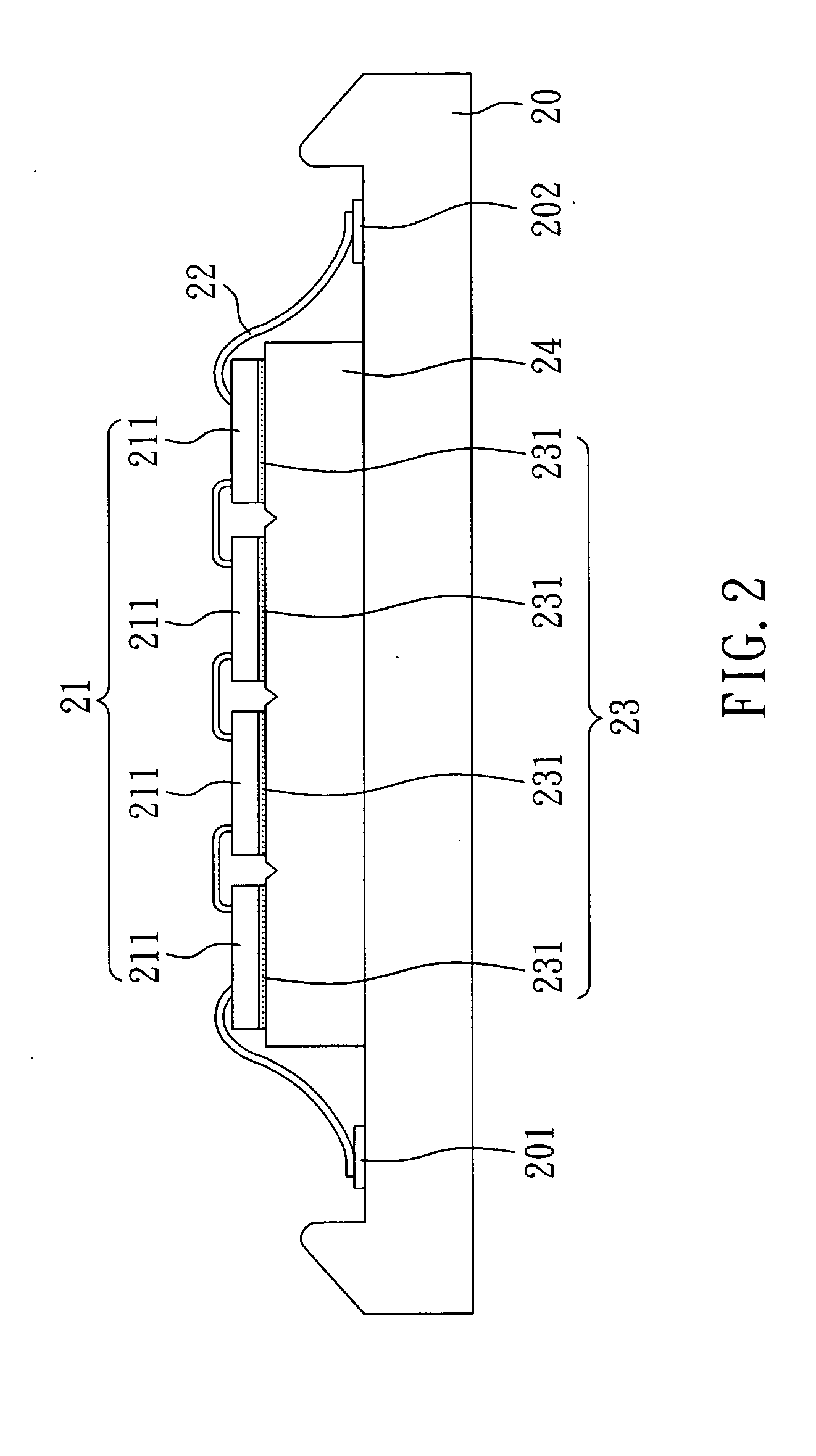
[0019]FIG. 2 is a perspective view of a packaging structure of AC LEDs of a preferred embodiment of the present invention.

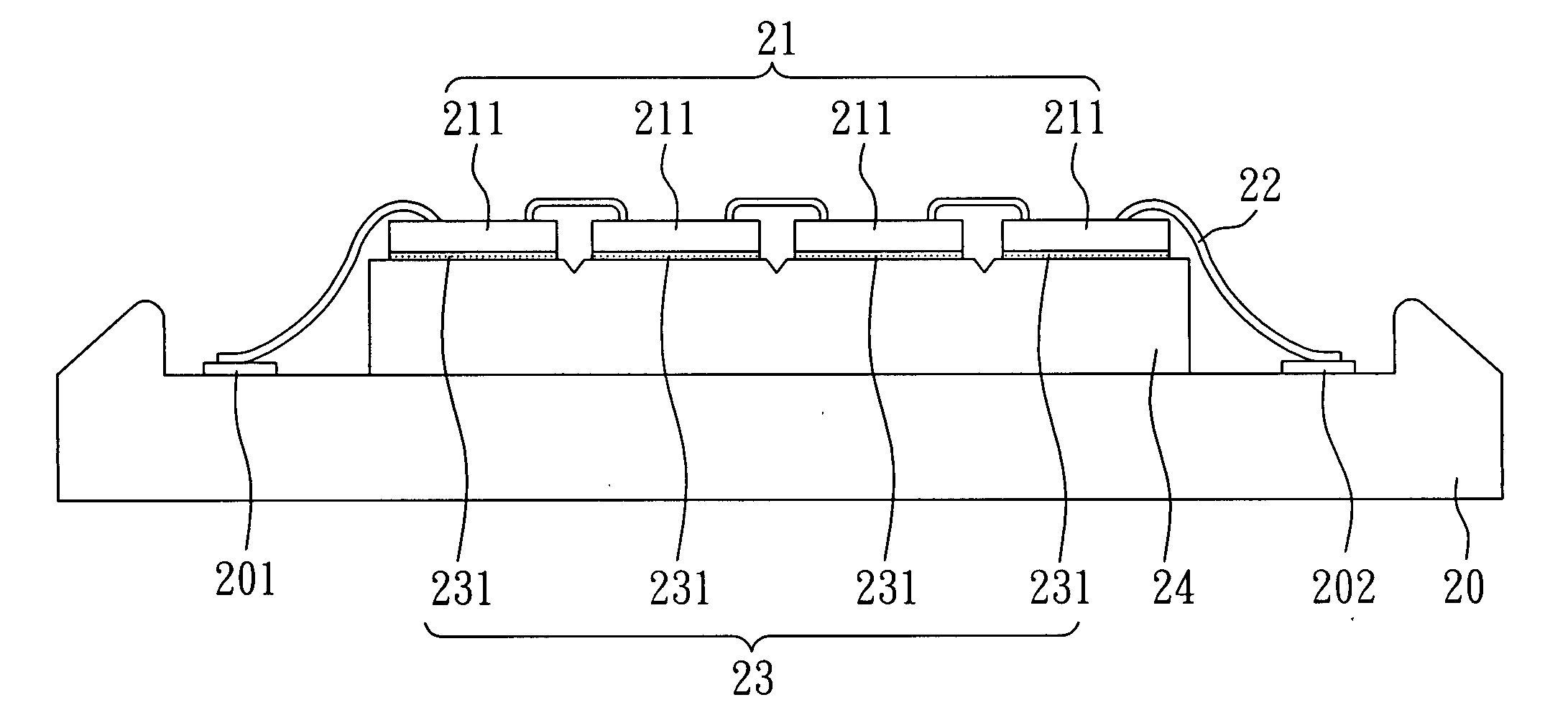
[0020]As shown in FIG. 2, the packaging structure of AC LEDs of the present embodiment comprises: a carrier 20, an AC LED module 21, and a die-bonding insulating layer 23. Herein, the carrier 20 contains a positive electrode connecting end 201, and a negative electrode connecting end 202. The AC LED module 21 is disposed on the carrier 20, wherein the AC LED module 21 electrically connects to the positive electrode connecting end 201 and the negative electrode connecting end 202 of the carrier 20. The die-bonding insulating layer 23 is disposed between the AC LED module 21 and the carrier 20.

[0021]In the present embodiment, the die-bonding insulating layer 23 is a die-bonding silicone layer. In addition, the thickness of the die-bonding insulating layer 23 may be 50˜120 μm. In the present embodiment, the thickness of the die-bonding insulating layer 23 is 80

[0022...


PUM


Abstract

A packaging structure of AC LEDs is provided, which comprises: a carrier containing a positive electrode connecting end, and a negative electrode connecting end; an AC LED module disposed on the carrier, wherein the AC LED module electrically connects to the positive electrode connecting end and the negative electrode connecting end of the carrier; and a die-bonding insulating layer disposed between the AC LED module and the carrier.

Description

BACKGROUND OF THE INVENTION[0001]1. Field of the Invention[0002]The present invention relates to a packaging structure of alternating current light-emitting diodes (AC LEDs) and, more particularly, to a packaging structure of AC LEDs with good reliability.[0003]2. Description of Related Art[0004]FIG. 1 is a perspective view of a conventional packaging structure of an LED. The conventional packaging structure of the LED comprises: a carrier 10, and an LED die 11. The LED die 11 electrically connects to a positive electrode connecting end 101 and a negative electrode connecting end 102 of the carrier 10 through conductive wires 12, and the LED die 11 is bound on the carrier through a conductive silver paste 13.[0005]When the LED die 11 is bound on the carrier 10 by use of the conductive silver paste 13, the conductive silver paste 13 may cover the edge of the LED die 11, and even totally cover the surface of the LED die 11. In this case, partial surface of the LED die 11 is covered, s...

Claims


Application Information

Patent Timeline
Patent Type & Authority Applications(United States)
IPC IPC(8): H01L33/62H01L33/48
CPCH01L25/0753H01L33/62H01L2224/45144H01L2224/48137H01L2224/73265H01L2224/48091H01L2924/00014H01L2924/00
Inventor HSU, HUI-WEN
Owner FORWARD ELECTRONICS CO LTD
Why Eureka
Try Eureka