Image display apparatus with image entry function

a display apparatus and image technology, applied in the field of image display apparatuses, can solve the problems of low accuracy, low transmission accuracy, difficult high-speed signal processing, etc., and achieve the effect of reducing the aperture ratio, increasing the current consumption, and lowering the screen brightness

Active Publication Date: 2008-08-21
PANASONIC LIQUID CRYSTAL DISPLAY CO LTD +1
View PDF11 Cites 85 Cited by
  • Summary
  • Abstract
  • Description
  • Claims
  • Application Information

AI Technical Summary

Benefits of technology

[0013](5) Further, in the above technology of the related art, each pixel requires elements including many thin film transistors, which lower the aperture ratio of the pixels that display images, and adding more pixels increases the current consumption. A drop in the aperture ratio lowers the screen brightness, and the increased power consumption shortens the operating time especially in the case of portable terminals. The switching elements vertically (perpendicularly, second direction) and in read line sequence read out the light leakage current from the multiple photo sensing elements arrayed to the side (horizontally, first direction) in the region defined by pixel select lines (gate lines), display data lines (signal lines, data lines) and read lines (sensing lines). So that the time needed to acquire a horizontal / vertical two-dimensional photo signal becomes longer as the number of photo sensor elements and switching elements is increased. The detection speed therefore slows down as the circuit density increases.
[0028](6) This invention is capable of high-speed detection without increasing the components or circuitry required in processing to correct the backlighting or temperature compensation. Moreover, this invention can reduce the backlighting power consumption by internalizing the photo sensor in the image display apparatus.

Problems solved by technology

Namely,(1) the first and the second photo sensors are installed on the edge of the display region or outside the display region and are therefore affected by variations in element characteristics or differences in temperature characteristics between the first and second photo sensor; so that the accuracy is low when sensing the state of external light on the center section of the display, etc.(2) The first, second, and third photo sensor are formed at installation positions away from each other which causes low transmission accuracy when sending detection signals due to differences in resistance among the signal lines sending each sensor's photo detection signals.(3) High speed signal processing is difficult because the signal scanner unit which is the peripheral circuit must convert the sensing signals for the photo sensor within the display device into decision signals, and a signal controller unit must convert them into control signals, and the sensitivity of the photo sensor within the panel screen must be adjusted.(4) Installing circuits such as the signal scanner unit and signal controller unit increases the peripheral circuit scale.(5) Further, in the above technology of the related art, each pixel requires elements including many thin film transistors, which lower the aperture ratio of the pixels that display images, and adding more pixels increases the current consumption.
A drop in the aperture ratio lowers the screen brightness, and the increased power consumption shortens the operating time especially in the case of portable terminals.

Method used


Image

  • Image display apparatus with image entry function
  • Image display apparatus with image entry function
  • Image display apparatus with image entry function

Examples


first embodiment

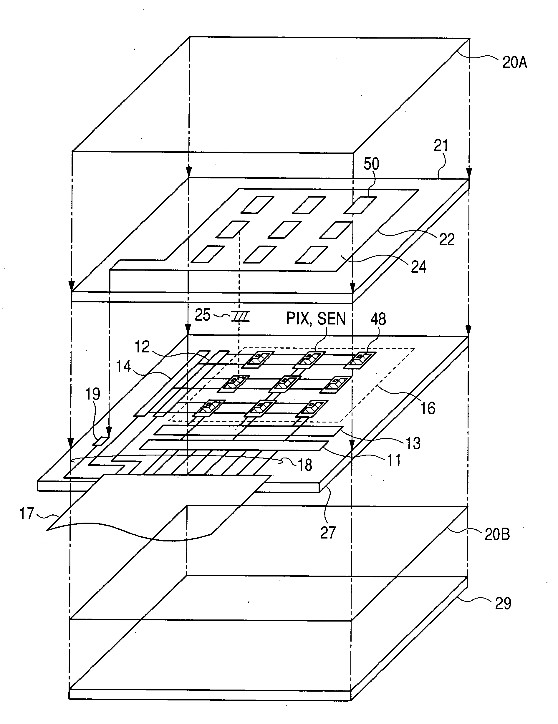
[0049]FIG. 1 is a perspective view of the liquid crystal display device with image entry function in the first embodiment of the image display apparatus of this invention. In this figure, a display region (pixel region) 16 formed from multiple pixels (shown by pixel electrode 48) arrayed in a matrix is contained on the main surface (inner surface made up of thin film transistors (TFT), etc.) of the lower glass substrate 27 serving as the first insulator substrate (TFT substrate). The pixel PIX making up the display region 16 contains a photo sensing function SEN along with a display function. The outer side of the pixel region 16 on the main surface of this glass substrate 27 contains: a data driver 11 connecting to the source electrode or the drain electrode (here, the source electrode) of the switching TFT (first thin film transistor, described later on) for pixel display, a gate driver 12 for applying a select signal to the gate electrode of the pixel switch TFT made up of pixels...

second embodiment

[0071]FIG. 9 is a block circuit diagram showing the image display apparatus of the second embodiment of this invention. The second embodiment differs from the first embodiment in the point that a photo sensor is formed in the image display apparatus made up of red, green and blue sub pixels. The other sections of the structure are identical to the first embodiment so a description of those identical sections is omitted. To simplify the description, the example given here utilizes a pixel circuit with two matrices each containing three sub pixels. The three color filters (red, green, blue) are fabricated on an opposing substrate (color filter board) and arrayed vertically in strips (top and bottom in FIG. 9).

[0072]By utilizing the characteristics described using FIGS. 8A and 8B, in the second embodiment, the TFT can detect the reflected light LREF from the user's touch by installing a first pixel PIXS containing a first photo sensor SENA for receiving external light input from the ob...

third embodiment

[0073]FIG. 10 is a block circuit diagram for describing the third embodiment of the image display apparatus of this invention. Compared to the second embodiment, the third embodiment differs in the point that a structure for horizontally (to the left and right in FIG. 10) outputting the detection signal has been added. Only this differing point is described here and a description of sections identical to the second embodiment is omitted. In FIG. 10, the first row of switching TFT 1 for red sub pixels are connected to data line DR, and the second row of switching TFT 2 for blue sub pixels are connected to the data line DB. Signals read out from the first row of red sub pixels and the second row of blue sub pixels can be sent to the X address detection circuit 13X by connecting these data lines are connected to the X address detection circuit (sensor signal processor circuit) 13X.

[0074]The switching TFT1 for the second row of red sub pixels connects to the read signal line R2, and the...


PUM


Abstract

An image display apparatus with image entry function capable of high-speed and high-accuracy direct screen entry without increasing the peripheral circuit scale or the number of circuit elements for each pixel that lower the pixel aperture ratio. A first pixel circuit and a second pixel circuit are alternately arrayed horizontally. First and second data lines are connected to a data driver and a sensor signal processor circuit. Selector switches are connected to the input terminal of the data driver. Gray scale voltages are sent from the data driver to the first and second data lines, and first and second photo sensor signals are sent to the sensor signal processor circuit.

Description

CLAIM OF PRIORITY[0001]The present application claims priority from Japanese application JP 2007-039181 filed on Feb. 20, 2007, the content of which is hereby incorporated by reference into this application.FIELD OF THE INVENTION[0002]The present invention relates to an image display apparatus with an internal photo sensor in the display panel and relates in particular to an image display apparatus with image entry function allowing high-speed, high accuracy direct screen input without lowering the pixel aperture ratio.BACKGROUND OF THE INVENTION[0003]Image display apparatus containing an image entry function allowing the user to enter information by touching the screen with fingers (hereafter simply called touch) are used in portable terminals such as PDA, and customer guidance terminals such as automated reception terminals. Image display apparatus containing this type of image entry functions utilize known methods including a method that detects the change in resistance in the (s...

Claims


Application Information

Patent Timeline
Patent Type & Authority Applications(United States)
IPC IPC(8): G06F3/042
CPCG06F3/0412G06F3/042
Inventor KINOSHITA, MASAYOSHIKAGEYAMA, HIROSHI
Owner PANASONIC LIQUID CRYSTAL DISPLAY CO LTD
Why Eureka
Try Eureka