Touch detection device and display device having touch sensor function

a technology of touch detection and display device, which is applied in the direction of instruments, computing, electric digital data processing, etc., can solve the problem of reducing the signal-to-noise ratio of detection signal

Active Publication Date: 2010-12-30
JAPAN DISPLAY INC
View PDF5 Cites 118 Cited by
  • Summary
  • Abstract
  • Description
  • Claims
  • Application Information

AI Technical Summary

Benefits of technology

[0010]However, the aforementioned touch panel (touch detection device) or the display device having a touch sensor function has the following disadvantages.
[0011]The touch detection device generates an electric variation on the sensor line in response to touch or detection of a detection target object (such as a user's finger or a stylus pen) to the detection surface without distinction of an optical type, a resistive film type, and an electrostatic capacitance type. Such an electric variation in the sensor line is detected in a leading end of the sensor line extending to the outer side from the detection surface. However, since the touch detection device generally demands a plurality of wiring lines in addition to the sensor line, the signal-to-noise (S / N) ratio of the detection signal decreases when the electric potential fluctuation in this wiring lines is overlapped on the sensor line as noise. A pixel circuit usually has an amplification function in an optical type, and an electric variation is relatively large in the resistive film type. On the contrary, in an electrostatic capacitance type touch detection device, the electric variation on the sensor line has a relatively small amplitude, and prevention of degradation of the S / N ratio of the detection signal is important, particularly, in the electrostatic capacitance type touch detection device.
[0012]Meanwhile, the display device having a touch sensor function makes progress from simply attaching a touch panel to the external surface of the display panel to forming an electrode for driving the touch sensor inside the display panel to achieve new objectives such as a thinner thickness and cost reduction. Therefore, a wiring line having a large voltage fluctuation functioning as noise source to the sensor line is frequently disposed in proximity of the sensor line in a thickness direction of the panel. Therefore, prevention of degradation in the S / N ratio of the detection signal becomes more important in the display device having a touch sensor function. Although this is a frequent case without distinction of the optical type, the resistive film type, or the electrostatic capacitance type, noise reduction in the sensor line is highly demanded particularly in the electrostatic capacitance type due to the aforementioned reason.
[0034]In the display device according to an embodiment of the present invention, the operational circuit performs an operation process using a line capacitance ratio for a plurality of outputs from a plurality of types of the sensor lines (or the sensing electrodes) that have a different line capacitance and neighbor to one another. As a result, the electric potential fluctuation component generated by the effect of the aforementioned other wiring lines (e.g., image signal lines) is effectively removed from the detection signal output from the operational circuit.

Problems solved by technology

However, since the touch detection device generally demands a plurality of wiring lines in addition to the sensor line, the signal-to-noise (S / N) ratio of the detection signal decreases when the electric potential fluctuation in this wiring lines is overlapped on the sensor line as noise.

Method used


Image

  • Touch detection device and display device having touch sensor function
  • Touch detection device and display device having touch sensor function
  • Touch detection device and display device having touch sensor function

Examples


first embodiment

1. First Embodiment

[0076][Basic Configuration and Operations for Touch-Sensing]

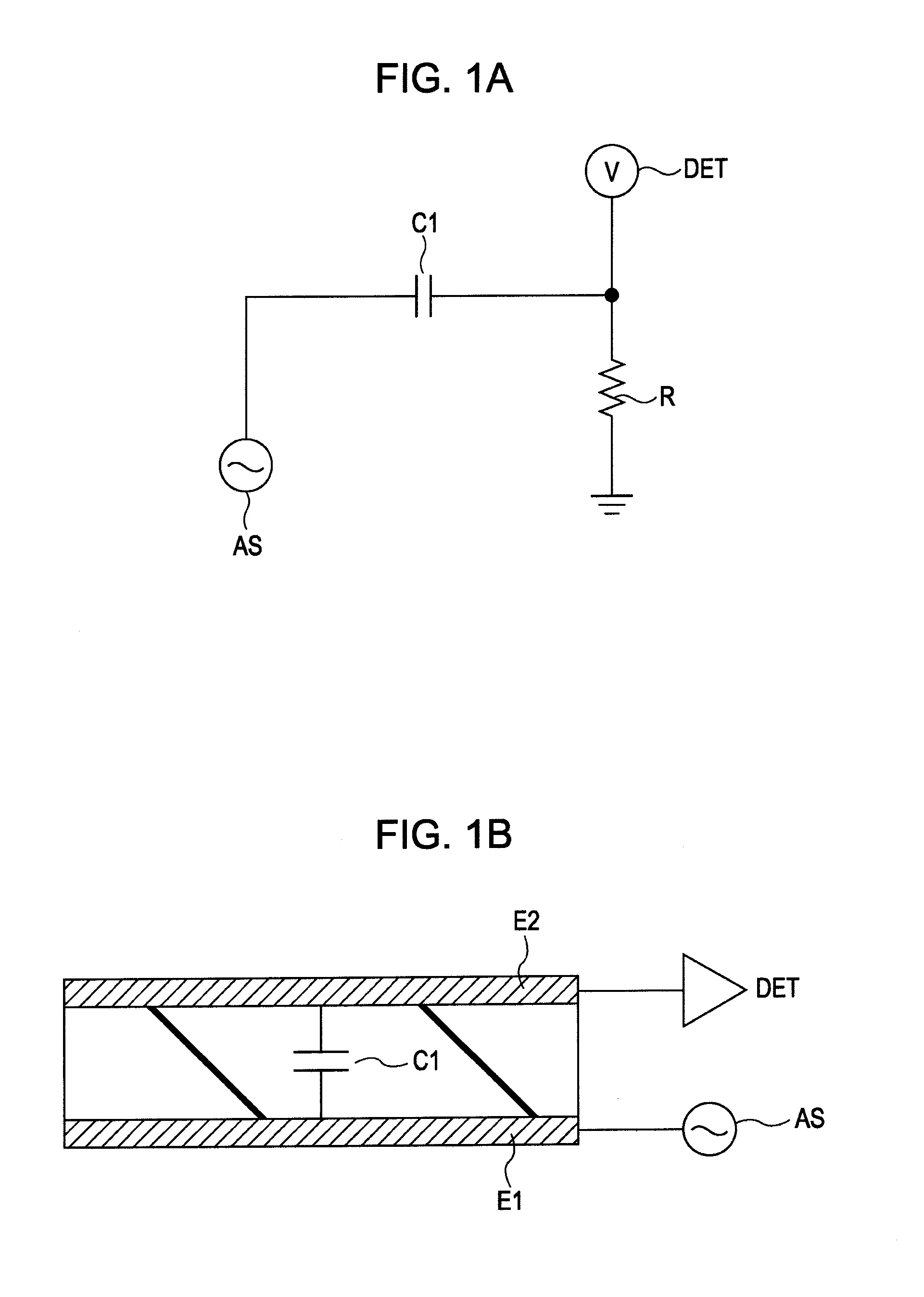
[0077]First, fundamentals of electrostatic capacitance element type touch-sensing will be described with reference to FIGS. 1A to 3C as assumptions of the first embodiment (common to other embodiments).

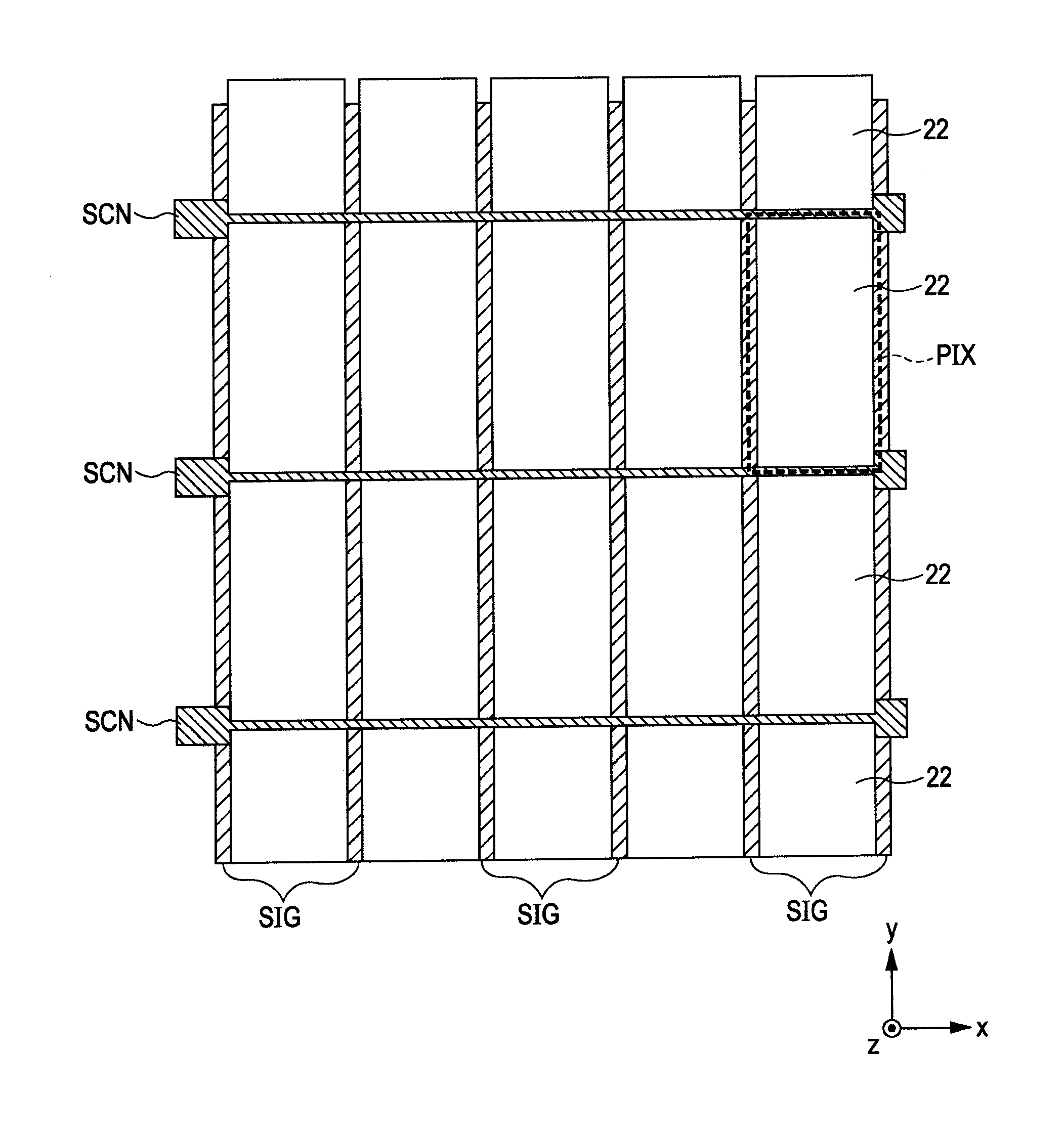
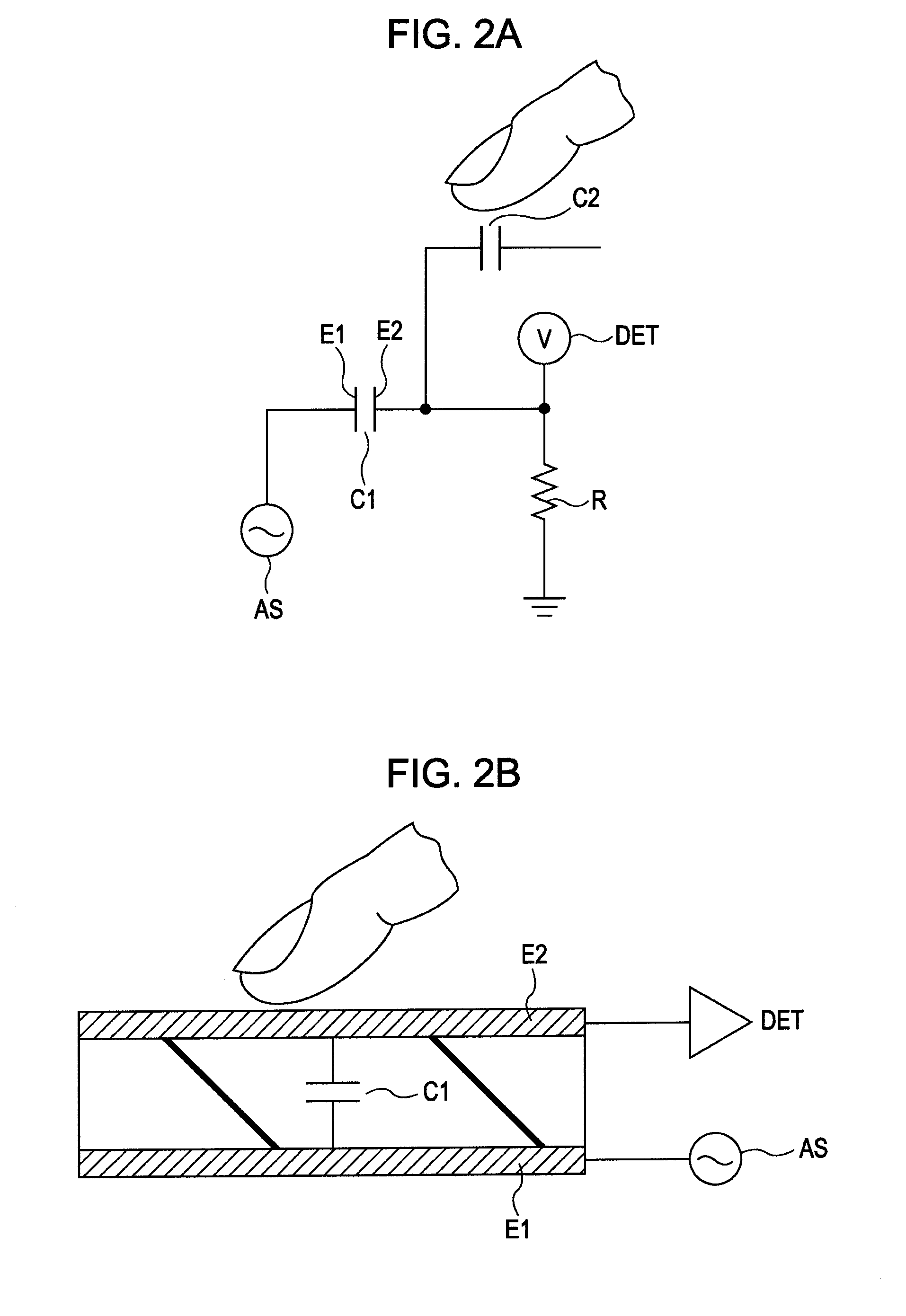
[0078]FIGS. 1A and 2A are equivalent circuit diagrams illustrating a touch sensor unit, and FIGS. 1B and 2B are constructional diagrams (schematic cross-sectional views) illustrating a touch sensor unit. Here, FIGS. 1A and 1B illustrate a case where a finger as a sensing target object is not in proximity of the sensor, and FIGS. 2A and 2B illustrate a case where a finger is disposed in proximity of or touches the sensor.

[0079]The illustrated touch sensor unit is an electrostatic capacitance type touch sensor and includes capacitance elements as shown in FIGS. 1B and 2B. Specifically, a capacitance element (electrostatic capacitance element) C1 includes a dielectric body D and a pair of electrodes arranged t...

first modification

2. First Modification

[0117]Here, another embodiment (modification) of changing the line capacitance ratio Kc will be described.

[0118]In the first modification, both the sensor lines have the same length, the same thickness, and the same material, but the width is different.

[0119]For example, a second sensor line having a width doubled by the first sensor line is considered. In this case, the line capacitance ratio Kc of the second sensor line against the first sensor line is approximately 2, and the denominator of the equation of FIG. 5C of the second sensor line becomes approximately a double of that of the first sensor line. In this case, if the widths of the m driving electrodes DEj are constant, the electrostatic capacitance Cp of the second sensor line becomes a double of that of the first sensor line. Therefore, in the first modification, the signal component (the crest value) of the detection signal becomes nearly the same between the first and second sensor lines.

second modification

3. Second Modification

[0120]In the second modification, both the sensor lines have the same thickness and material, but the length and the width are different.

[0121]For example, as shown in FIGS. 4A and 4B, it is assumed that the length of the short sensor line is a half (½) of the length of the long sensor line, and the width of the short sensor line is a half (½) of the width of the long sensor line. In this case, the denominator of the equation of FIG. 5C of the short sensor line becomes a quarter (¼) of that of the long sensor line (the line capacitance ratio Kc is 4 or ¼). In addition, the electrostatic capacitance Cp of the short sensor line becomes approximately a half (½) of that of the long sensor line. Therefore, in the second modification, the signal component (the crest value) of the detection signal output from the short sensor line becomes approximately a double of the signal component (the crest value) of the detection signal output from the long sensor line.


PUM


Abstract

A touch detection device includes: a detection surface; a plurality of sensor lines formed from a plurality of types of wiring lines having a different line capacitance; and a touch detection unit which detects an electric variation generated in a plurality of the sensor lines in response to touch or proximity of a detection target object to the detection surface, wherein the touch detection unit has an operational circuit for generating a detection signal representing the electric variation by performing an operation process using a line capacitance ratio for a plurality of outputs from a plurality of types of the sensor lines neighboring to one another with a different line capacitance.

Description

[0001]The present application claims priority to Japanese Patent Application No. JP 2009-155188 filed in the Japanese Patent Office on Jun. 30, 2009, the entire content of which is hereby incorporated by reference.BACKGROUND OF THE INVENTION[0002]1. Field of the Invention[0003]The present invention relates to a touch detection device for detecting touch or proximity of a user's finger or a pen to a detection surface. In addition, the present invention relates to a display device having a function of the touch detection device (touch sensor).[0004]2. Description of the Related Art[0005]In general, a touch detection device is a device for detecting touch or proximity of a user's finger or a pen to a detection surface.[0006]A display device is known in the art, which allows a user to input information instead of typical buttons by overlappingly forming a touch detection device called a touch panel on a display panel and displaying various buttons as an image on a display surface. When ...

Claims


Application Information

Patent Timeline
Patent Type & Authority Applications(United States)
IPC IPC(8): G06F3/045
CPCG06F3/044G06F3/04166G06F3/0445G06F3/0446G06F3/0412G06F3/047G06F2203/04106G06F2203/04108G06F2203/04112
Inventor ISHIZAKI, KOJINOGUCHI, KOUJITAKEUCHI, TAKEYANAKANISHI, TAKAYUKITERANISHI, YASUYUKI
Owner JAPAN DISPLAY INC
Why Eureka
Try Eureka