Light emitting device and display device

a technology of light emitting devices and display devices, which is applied in the direction of static indicating devices, instruments, electroluminescent light sources, etc., can solve the problems of inability to drive the data line with a high speed, the number of gradations that can be displayed is limited, and the difficulty of output a large amplitude data signal, etc., to reduce the power consumption of the device, and effectively represent a multi-gradation

Active Publication Date: 2005-02-03
SANYO ELECTRIC CO LTD
View PDF4 Cites 19 Cited by
  • Summary
  • Abstract
  • Description
  • Claims
  • Application Information

AI Technical Summary

Benefits of technology

[0018] As described, according to the present invention, it is not necessary to directly control an operation of a driver transistor for controlling, with a digital data signal, supply of power to a display element such as, for example, an organic EL element (power supply operation). With the present invention, the digital data signal is only required to control the operation of the control transistor, that is, switching on and off of the control transistor, to control whether or not the gate potential of the driver transistor is to be fixed to a predetermined potential such as a power supply. In other words, the digital data signal only needs an amplitude for controlling switching on and off of the control transistor and, thus, the amplitude can be reduced compared to a structure in which the operation of the driver transistor is directly controlled. Therefore, it is possible to employ a simple circuit at the processor and output sections for a data signal and the power consumption can be reduced.
[0019] In addition, because it is possible to drive the device using a digital data signal having a smaller amplitude, for example, a voltage resistance and a charge supply capability of the selection transistor in each pixel placed on a signal supply route of the digital data signal need not be significantly increased. In addition, even when a storage capacitor for storing a voltage corresponding to the digital data signal for a predetermined period is to be provided, it is possible to use a capacitor with a small capacitance. These transistor and storage capacitor correspond to parasitic capacitances (capacity load) electrically connected to the data line. With the present invention, it is possible to reduce the parasitic capacitance, and thus, it is easy to increase the transfer speed of the data signal. As a result, the requirements for increasing the number of display gradations are simplified.
[0021] Moreover, the subfield period may be correlated to each bit of the digital data signal, and a signal having a pulse width corresponding to an element operation period within each subfield period can be supplied to the control line as a control pulse signal. In this structure, it is possible to effectively represent a multi-gradation by assigning weights to each bit in the digital data. It is possible to set the element operation period (light emission period or display period), that is, the pulse width of the control pulse signal, during the subfield period to a width corresponding to a bit of the digital data signal, more specifically, the digit of the bit to accommodate this configuration.
[0022] The amplitude of the control pulse signal (in particular, level of the pulse signal) may be set to an amplitude necessary to shift the gate potential of the driver transistor when the potential is not fixed by the control transistor and to switch on and off the power supply operation to the emissive element by the driver transistor around the shifting operation. The control pulse signal is common to all pixels and is required to be output only once each subfield period, and, even when the amplitude of the control pulse signal is large, because the frequency as a pulse signal is low, it is possible to inhibit an increase in the power consumption.
[0023] As described, according to the present invention, in a device which emits light for which achieves a display based on digital data, it is only necessary to supply a digital data signal of a minimum amplitude to a data line in which the parasitic capacitance is maintained low, and thus, it is possible to employ a simple driver circuit to realize such a device. Because of this, it is also possible to reduce the power consumption of the device.
[0024] Moreover, because it is possible to output a digital data signal at a high speed, a multi-gradation display can be achieved and it is possible to further increase the number of gradations.

Problems solved by technology

However, as described above, the parasitic capacitance connected to the data line to which the data signal is to be output is large, and, thus, it is difficult to output a data signal having a large amplitude to allow sufficient control to switch on and off the driver transistor 22 with a sufficiently high speed, to the data line to which a large parasitic capacitance is connected.
Therefore, it is not possible to drive the data line with a high speed in order to increase the number of display gradations and the number of gradations that can be displayed is limited.

Method used


Image

  • Light emitting device and display device
  • Light emitting device and display device
  • Light emitting device and display device

Examples


Embodiment Construction

[0028] A preferred embodiment of the present invention will now be described referring to the drawings.

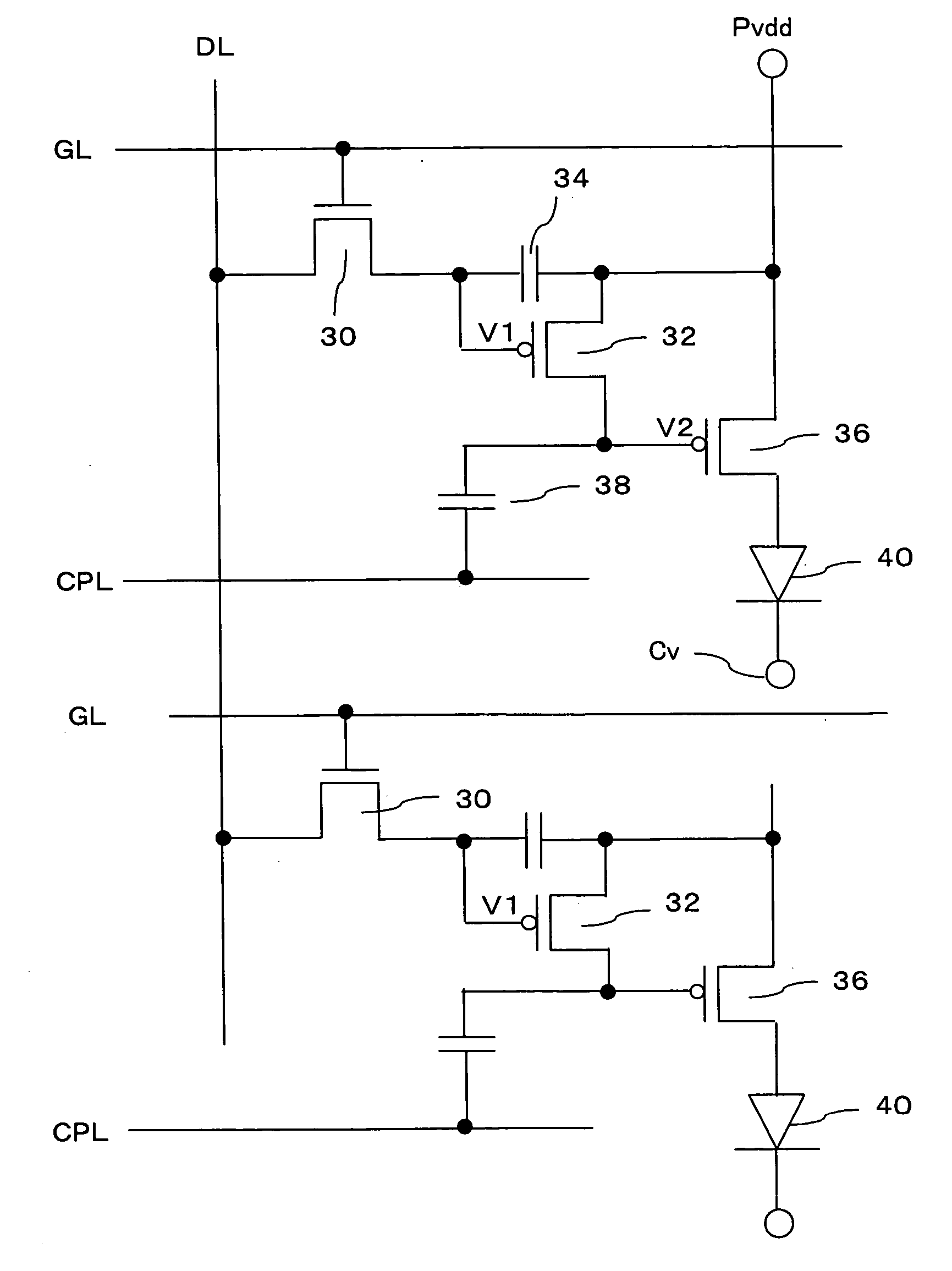
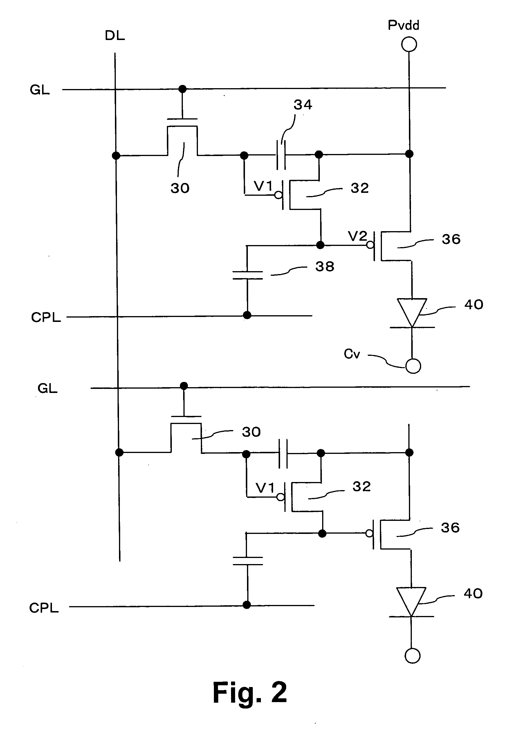
[0029]FIG. 2 shows an equivalent circuit showing a pixel among a plurality of pixels arranged in a matrix form in a display region according to a preferred embodiment of the present invention.

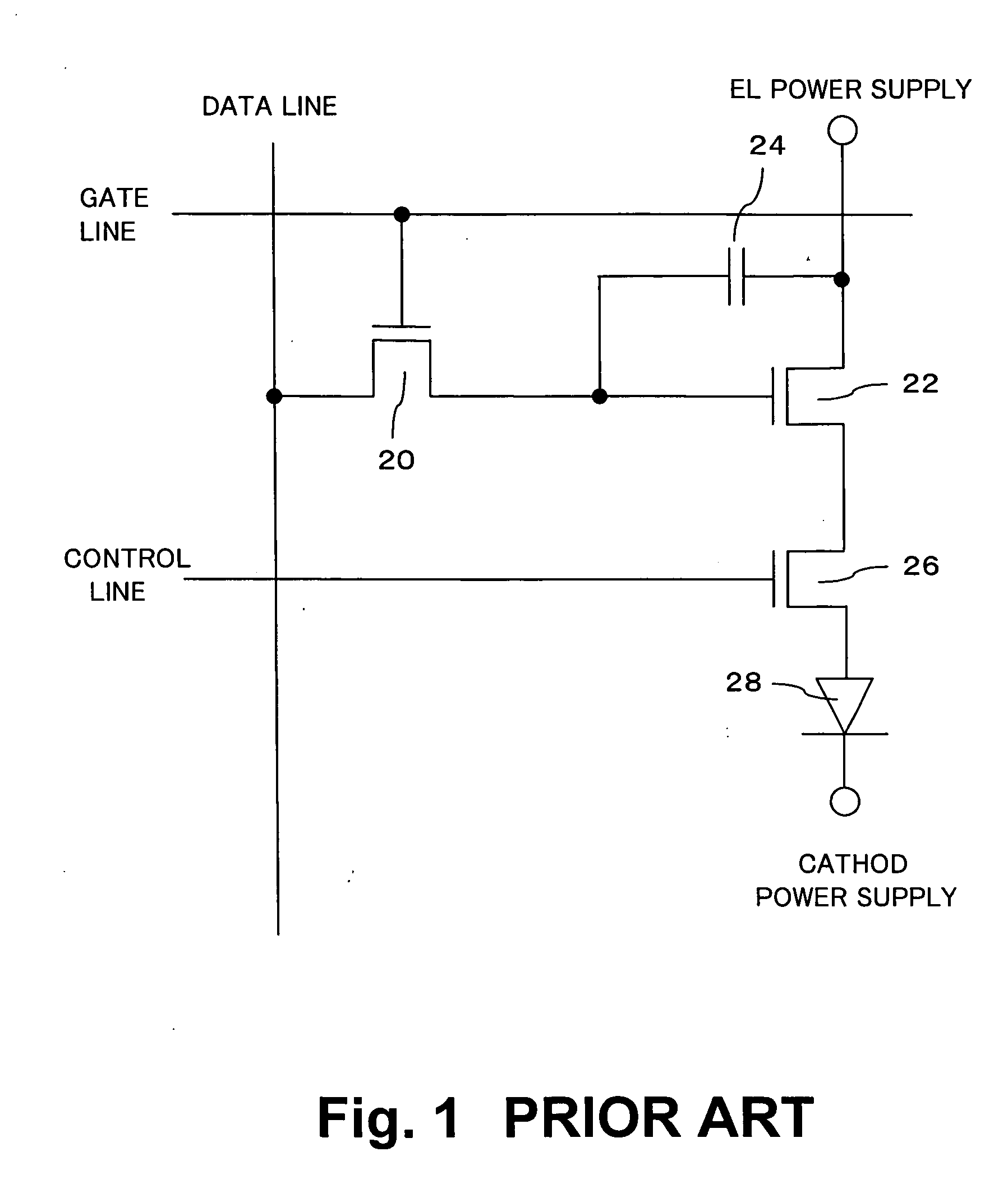
[0030] In the structure illustrated in FIG. 2, each pixel comprises an organic EL element 40. Each pixel further has a selection transistor (switching transistor; hereinafter also referred to as a “selection TFT”) 30, a storage capacitor 34, a control transistor (control TFT) 32, a driver transistor (driver TFT) 36, and a control capacitor 38 for controlling light emitting operation of the organic EL element 40. In addition, a data line DL extending along a vertical scan direction and for supplying a digital data signal to corresponding pixels, a selection line (gate line) extending along a horizontal scan direction and for outputting a selection signal (gate signal) for selecting pixels arr...


PUM


Abstract

Each pixel in a display device includes an emissive element, a driver transistor, a control transistor, and a control capacitor. The driver transistor is provided between the emissive element and a power supply and controls supply of power from the power supply to the emissive element. The control transistor is connected between a constant voltage power supply and a gate of the driver transistor, receives a digital data signal on a gate, and controls whether or not to fix a gate voltage of the driver transistor. The control capacitor is connected between a control line and the gate of the driver transistor. The gate voltage of the driver transistor is shifted to a voltage corresponding to a control pulse signal when the control transistor is off and is non-fixed during a light emission period defined by the control pulse signal applied to the control line.

Description

CROSS-REFERENCE TO RELATED APPLICATIONS [0001] The Japanese priority applications Numbers 2003-177267 and 2004-170835 upon which this patent application is based are hereby incorporated by reference. BACKGROUND OF THE INVENTION [0002] 1. Field of the Invention [0003] The present invention relates to a display device, and in particular to a digital display device having a display element such as an emissive element in each pixel and in which the elements are operated using digital signals to represent gradations. [0004] 2. Description of the Related Art [0005] Because electroluminescence (hereinafter simply referred to as “EL”) display devices in which a self-emitting EL element, for example, is used as an emissive element in each pixel have advantages such as that the device is thin, self-emitting, and consumes less power, EL display devices have attracted much attention as alternatives to display devices such as liquid crystal display (LCD) and cathode ray tube (CRT) display device...

Claims


Application Information

Patent Timeline
Patent Type & Authority Applications(United States)
IPC IPC(8): G09G3/20H05B44/00G09G3/30G09G3/32G09G5/00H01L51/50H05B33/00H05B33/14
CPCG09G3/2022G09G3/3233G09G2300/0852G09G2330/021G09G2300/0876G09G2310/06G09G2320/043G09G2300/0861G09G3/30H05B33/00
Inventor SANO, KEIICHI
Owner SANYO ELECTRIC CO LTD
Why Eureka
Try Eureka