

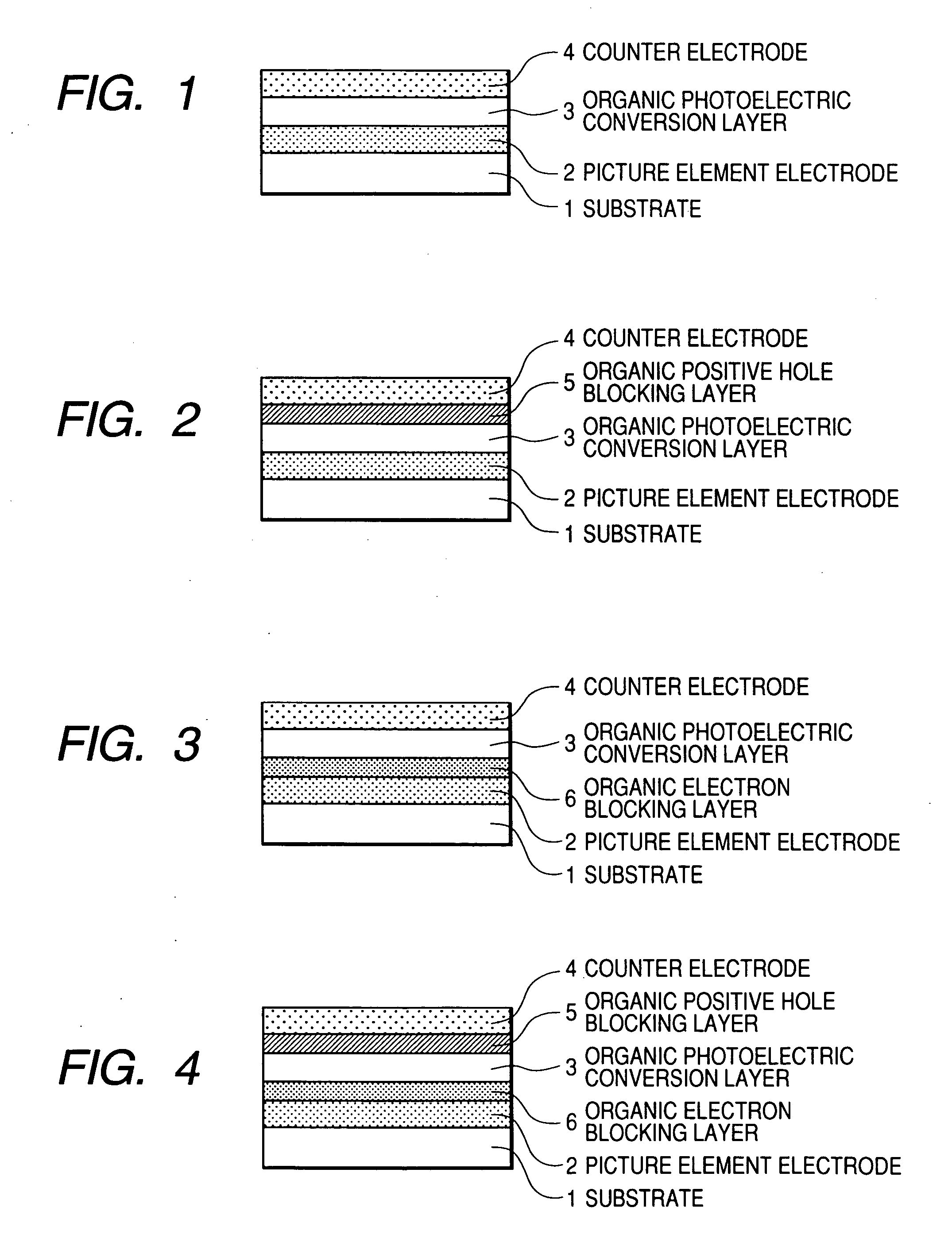
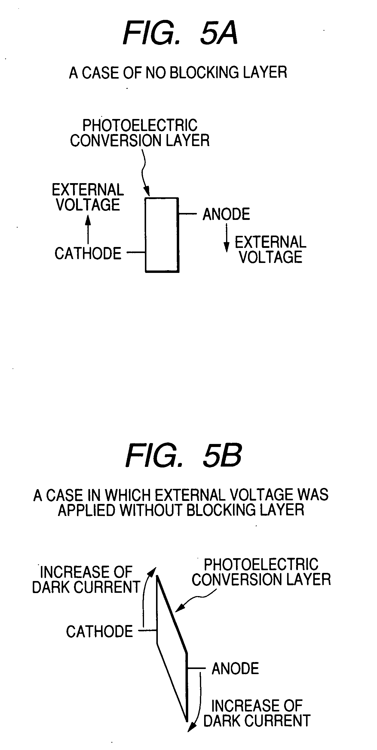
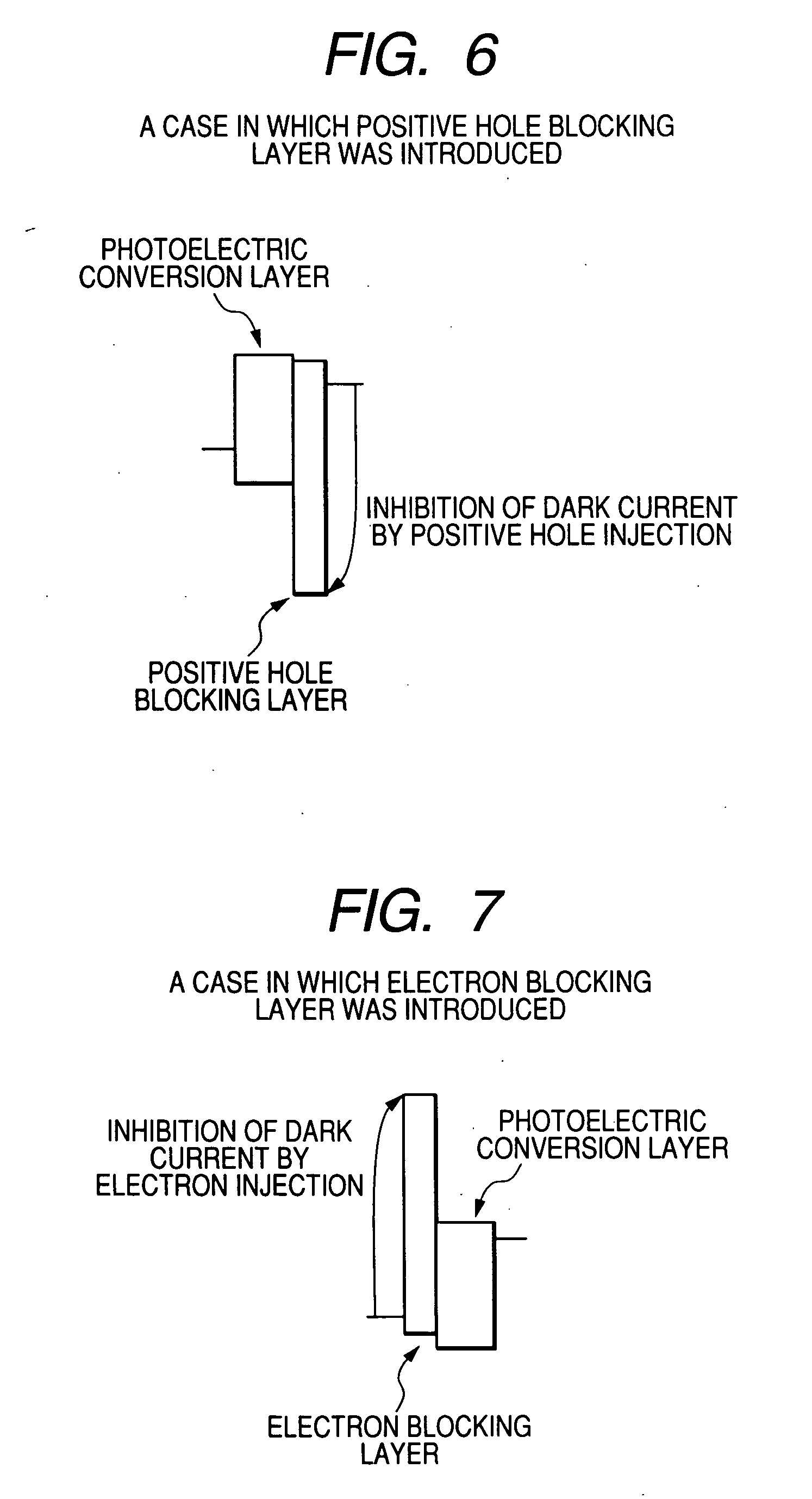
Organic photoelectric conversion element and image element
a photoelectric conversion element and organic technology, applied in the field of organic photoelectric conversion elements, can solve the problems of reducing the s/n ratio, increasing the photoelectric conversion efficiency, and reducing the efficiency generated by the insertion of the blocking layer, so as to improve the speed of response, improve the photoelectric conversion efficiency, and improve the effect of photoelectric conversion efficiency
- Summary
- Abstract
- Description
- Claims
- Application Information
AI Technical Summary
Benefits of technology
Problems solved by technology
Method used
Image

Examples
example 4
[0163] The procedure of Example 1 was repeated, except that 1% of BEDT-TTF (mfd. by Tokyo Kasei, sublimation-purified) was simultaneously co-deposited when HB-1 was deposited.
[0164] BEDT-TTF (Doping Material to Positive Hole Blocking Layer)
example 5
[0165] The procedure of Example 2 was repeated, except that 1% of F4TCNQ (mfd. by Tokyo Kasei, sublimation-purified) was simultaneously co-deposited when EB-l was deposited.
[0166] F4TCNQ (Doping Material to Electron Blocking Layer)
Comparative Example 1 (FIG. 13)
[0167] A film of PR-122 was formed under the same conditions as in Example 1 on a substrate equipped with ITO which had been washed in the same manner as in Example 1, this substrate was subsequently transferred into a metal deposition chamber to carry out deposition of A1 and further sealed, and then measurement of light current, dark current and IPCE was carried out.
Comparative Example 2 (FIG. 14)
[0168] Preparation of an element and evaluation of its performance were carried out under the same conditions of Example 1, except that Alq3 (mfd. by NIPPON STEEL CORP, sublimation-purified) (Ea: 3.0 eV, Ip: 5.8 eV) was used instead of HB-1.
[0169] Alq3 (Positive Hole Blocking Material)
Comparative Example 3 (FIG. 15)
[0170]...
PUM
| Property | Measurement | Unit |
|---|---|---|
| ionization potential | aaaaa | aaaaa |
| thickness | aaaaa | aaaaa |
| depth | aaaaa | aaaaa |
Abstract
Description
Claims
Application Information