Photoelectric conversion element, method for producing photoelectric conversion element, and solid-state imaging device

a technology of photoelectric conversion element and conversion method, which is applied in the direction of sustainable manufacturing/processing, television systems, radio frequency controlled devices, etc., can solve the problems of reducing the efficiency effect and difficulty in applying the technique of improving photoelectric conversion efficiency, so as to improve the photoelectric conversion efficiency and suppress the generation of dark current

Active Publication Date: 2009-02-26
FUJIFILM CORP
View PDF4 Cites 59 Cited by
  • Summary
  • Abstract
  • Description
  • Claims
  • Application Information

AI Technical Summary

Benefits of technology

[0014]An object of the invention is to provide a photoelectric conversion element, which can improve the photoelectric conversion efficiency with suppressing generation of dark current; a method for producing the photoelectric conversion element, and a solid-state imaging device.
[0015]As is described above, it has been difficult to apply the technique of improving photoelectric conversion efficiency by using fullerene, which has been examined with solar cells, as such to the imaging device, and further investigations are required. Thus, as a result of various investigations, the inventors have found that by sufficiently reducing the mixing ratio of fullerene, both improvement of the efficiency by fullerene and reduction of dark current can be attained at the same time to thereby obtain a sufficient photo current / dark current ratio. It has usually been considered that, when the mixing ratio of fullerene is reduced, there results a reduced effect of improving the efficiency. However, it has now been found that, when a voltage is applied from outside, surprisingly enough, the effect is not reduced so much, while the dark current is remarkably reduced. As a result, an imaging device can be provided with an enough photo current / dark current ratio.
[0016]Also, the broad absorption spectrum due to fullerene can be narrowed by reducing the mixing ratio of fullerene, and thus it becomes possible to apply the element to an imaging device.

Problems solved by technology

As is described above, it has been difficult to apply the technique of improving photoelectric conversion efficiency by using fullerene, which has been examined with solar cells, as such to the imaging device, and further investigations are required.
It has usually been considered that, when the mixing ratio of fullerene is reduced, there results a reduced effect of improving the efficiency.

Method used


Image

  • Photoelectric conversion element, method for producing photoelectric conversion element, and solid-state imaging device
  • Photoelectric conversion element, method for producing photoelectric conversion element, and solid-state imaging device
  • Photoelectric conversion element, method for producing photoelectric conversion element, and solid-state imaging device

Examples


first embodiment

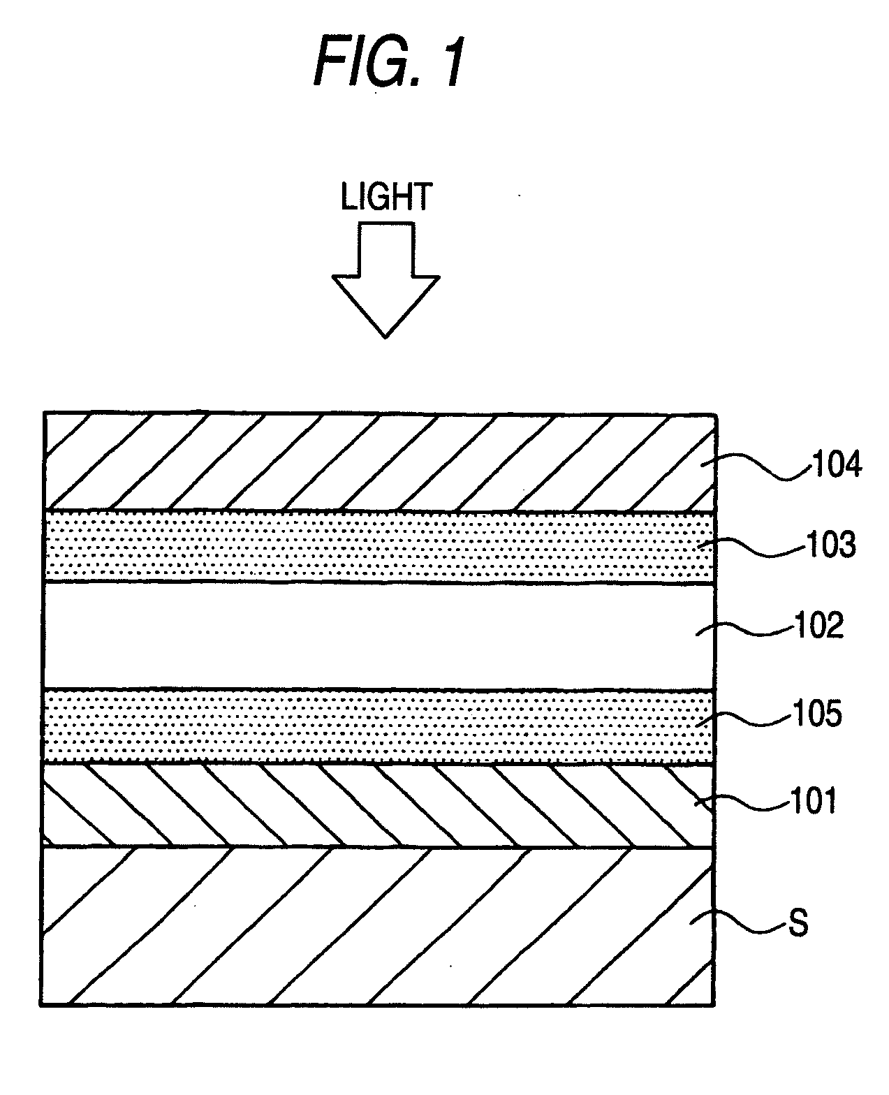
[0048]FIG. 1 is a schematic cross-sectional view showing a fundamental structure of a photoelectric conversion element of a first exemplary embodiment of the invention.

[0049]The photoelectric conversion element shown in FIG. 1 includes a substrate S, a lower electrode 101 (pixel electrode) formed on the substrate S, an electron-blocking layer 105 formed on the lower electrode 101, a photoelectric conversion layer 102 formed on the electron-blocking layer 105, a hole-blocking layer 103 formed on the photoelectric conversion layer 102, and an upper electrode 104 (opposing electrode) formed on the hole-blocking layer 103.

[0050]The photoelectric conversion layer 102 includes an organic material having the ability of photoelectric conversion. As the organic material, various organic semiconductor materials used in, for example, photosensitive materials for electrophotography may be used. Of them, materials having a quinacridone structure or organic materials having a phthalocyanine struc...

second embodiment

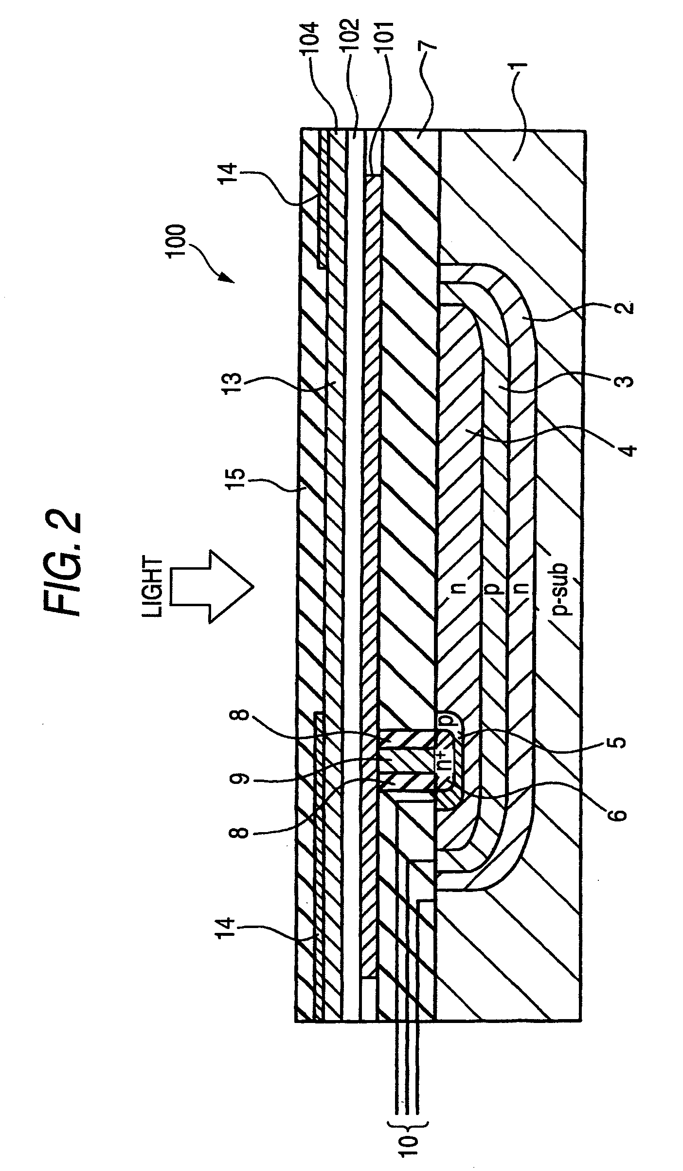
[0078]FIG. 2 is a cross-sectional schematic view showing one pixel of a solid-state imaging device for illustrating a second exemplary embodiment of the invention. In FIG. 2, the same reference numerals and signs are applied to the same structural members as those in FIG. 1.

[0079]In a solid-state imaging device 100, a number of pixels shown in FIG. 2 are arranged on the same plane in an array pattern, and data on one pixel of an image data can be generated by a signal obtained from the one pixel.

[0080]One pixel of the solid-state imaging device shown in FIG. 2 includes: a p-type silicon substrate 1; a transparent insulating film 7 formed on the p-type silicon substrate 1; a photoelectric conversion element of the structure described in the first embodiment including a lower electrode 101 formed on the insulating film 7, a photoelectric conversion layer 102 formed on the lower electrode 101, a hole-blocking layer 103 (not shown) formed on the photoelectric conversion layer 102, an el...

third embodiment

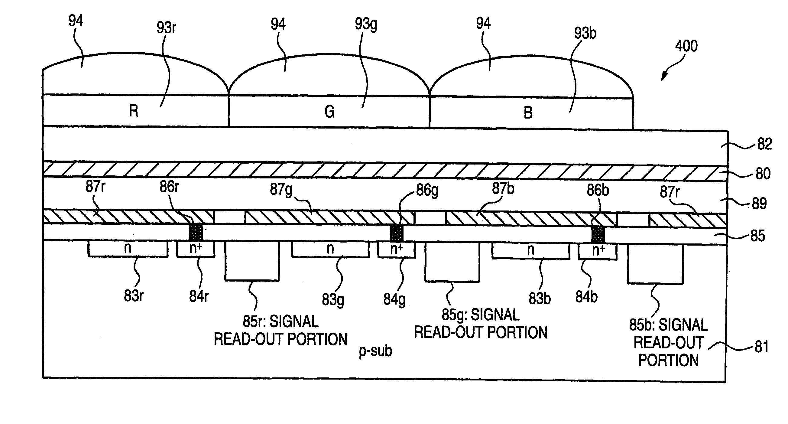
[0088]In this embodiment, two photodiodes are not stacked in the silicon substrate 1 shown in FIG. 2, but are arranged in the direction perpendicular to the incident direction of light to detect two colors of the light in the p-type silicon substrate.

[0089]FIG. 3 is a cross-sectional schematic view showing one pixel of a solid-state imaging device for illustrating a third exemplary embodiment of the invention. In FIG. 3, the same reference numerals and signs are applied to the same structural members as those in FIG. 1.

[0090]One pixel of the solid-state imaging device 200 shown in FIG. 3 includes a p-type silicon substrate 17, and a photoelectric conversion element of the structure described in the first embodiment including a lower electrode 101 formed above the p-type silicon substrate 17, a photoelectric conversion layer 102 formed on the lower electrode 101, a hole-blocking layer 103 (not shown) formed on the photoelectric conversion layer 102, an electron-blocking layer 105 (no...


PUM


Abstract

A photoelectric conversion element is provided and includes a photoelectric conversion portion. The photoelectric conversion portion includes: a pair of electrodes; and a photoelectric conversion layer between the pair of electrodes, and at least part of the photoelectric conversion layer includes a mixed layer of a p-type organic semiconductor and a fullerene, and a mixing ratio of the fullerene to the p-type organic semiconductor in terms of thickness ratio is less than 1:1.

Description

[0001]This application is based on and claims priority under 35 U.S.C. §119 from Japanese Patent Application No. 2007-215715 filed Aug. 22, 2007, the entire disclosure of which is herein incorporated by reference.BACKGROUND OF THE INVENTION[0002]1. Field of the Invention[0003]The present invention relates to a photoelectric conversion element including: a lower electrode; an upper electrode opposite to the lower electrode; and an organic photoelectric conversion layer formed between the lower electrode and the upper electrode, a method for producing the photoelectric conversion element, and a solid-state imaging device.[0004]2. Description of Related Art[0005]Photosensors are generally devices prepared by forming a photodiode (PD) in a semiconductor substrate such as silicon (Si) and, as a solid-state imaging device, a plane type solid-state imaging device is widely used in which PDs are two-dimensionally arranged in a semiconductor substrate, and signals each corresponding to a sig...

Claims


Application Information

Patent Timeline
Patent Type & Authority Applications(United States)
IPC IPC(8): H01L51/00H01L21/00H01L27/146H01L31/10H01L51/42H04N5/335H04N5/361H04N5/369
CPCB82Y10/00H01L27/302H01L27/307H01L51/0046H01L51/0059Y02E10/549H01L51/0078H01L51/0081H01L51/4246H01L51/4253H01L51/0071Y02P70/50H10K30/57H10K39/32H10K85/211H10K85/631H10K85/311H10K85/657H10K85/324H10K30/211H10K30/30
Inventor HAYASHI, MASAYUKI
Owner FUJIFILM CORP
Why Eureka
Try Eureka