Light-emitting device, method for manufacturing the same, and cellular phone

a technology of light-emitting devices and cellular phones, which is applied in the direction of discharge tube luminescnet screens, sustainable manufacturing/processing, and final product manufacturing, etc., can solve the problems of long manufacturing time, high manufacturing cost, and defective coverage, and achieve the effect of relaxing stress

Active Publication Date: 2013-12-17
SEMICON ENERGY LAB CO LTD
View PDF87 Cites 98 Cited by
  • Summary
  • Abstract
  • Description
  • Claims
  • Application Information

AI Technical Summary

Benefits of technology

[0008]Other problems that occur when a semiconductor circuit for driving a light-emitting element is formed and then the light-emitting element is formed thereover are long manufacturing time and high manufacturing cost.
[0026]Accordingly, the semiconductor circuit is not formed below the light-emitting element and thus the generation of defective coverage due to steps can be suppressed.
[0027]In addition, because a desiccant can be disposed in the space portion between the light-emitting element and the semiconductor circuit for driving the light-emitting element, the entry of moisture into the light-emitting layer can be prevented.
[0029]Furthermore, because a space (a space portion) is provided between the light-emitting element and the semiconductor circuit for driving the light-emitting element which are disposed over flexible substrates, stress can be relaxed even when the flexible substrates are bent.

Problems solved by technology

As mentioned above, one of problems is that defective coverage may be caused by a step or the like resulting from an element, a wiring, or the like that is formed below a light-emitting element.
Other problems that occur when a semiconductor circuit for driving a light-emitting element is formed and then the light-emitting element is formed thereover are long manufacturing time and high manufacturing cost.
Another problem is that a light-emitting layer in a light-emitting element is sensitive to moisture, so that the entry of moisture into a light-emitting element should be prevented.
In addition, a problem that occurs when a light-emitting element and a semiconductor circuit for driving the light-emitting element are formed over a hard substrate such as a glass substrate is that the light-emitting element and the semiconductor circuit cannot be incorporated into electronic devices of various shapes because such a hard substrate lacks flexibility and the shape cannot be changed.

Method used


Image

  • Light-emitting device, method for manufacturing the same, and cellular phone
  • Light-emitting device, method for manufacturing the same, and cellular phone
  • Light-emitting device, method for manufacturing the same, and cellular phone

Examples


embodiment 1

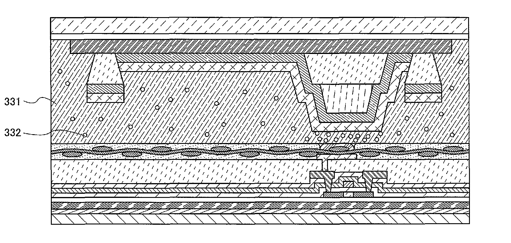
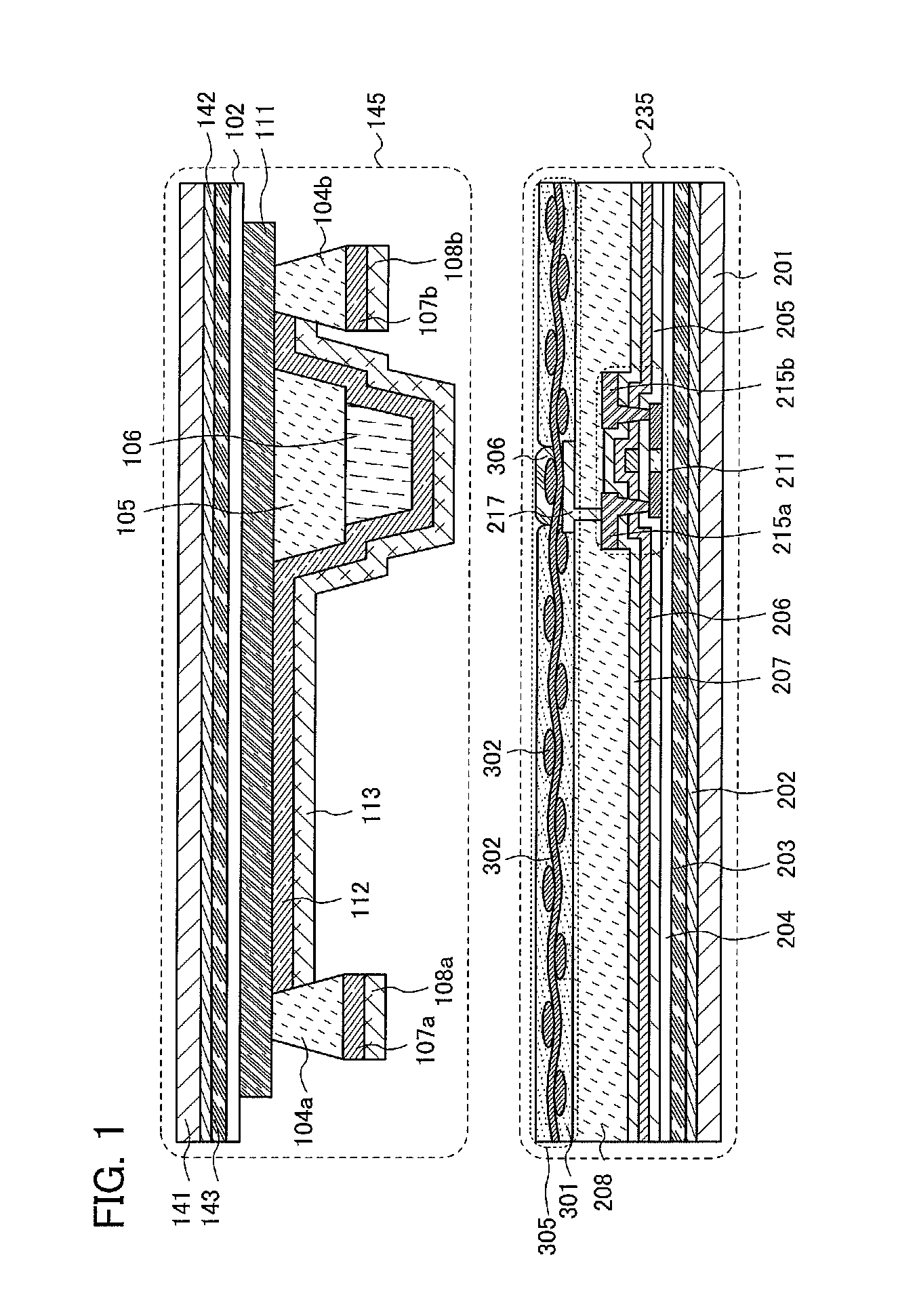
[0061]In this embodiment, a light-emitting device and a method for manufacturing the light-emitting device are described with reference to FIG. 1, FIGS. 2A to 2C, FIGS. 3A and 3B, FIGS. 4A and 4B, FIGS. 5A and 5B, FIGS. 6A to 6C, FIGS. 7A to 7D, FIGS. 8A to 8C, FIGS. 9A to 9C, FIGS. 10A and 10B, FIG. 11, FIG. 12, FIGS. 14A and 14B, FIG. 15, FIG. 16, FIGS. 17A and 17B, FIGS. 18A and 18B, FIG. 19, FIG. 20, and FIG. 21.

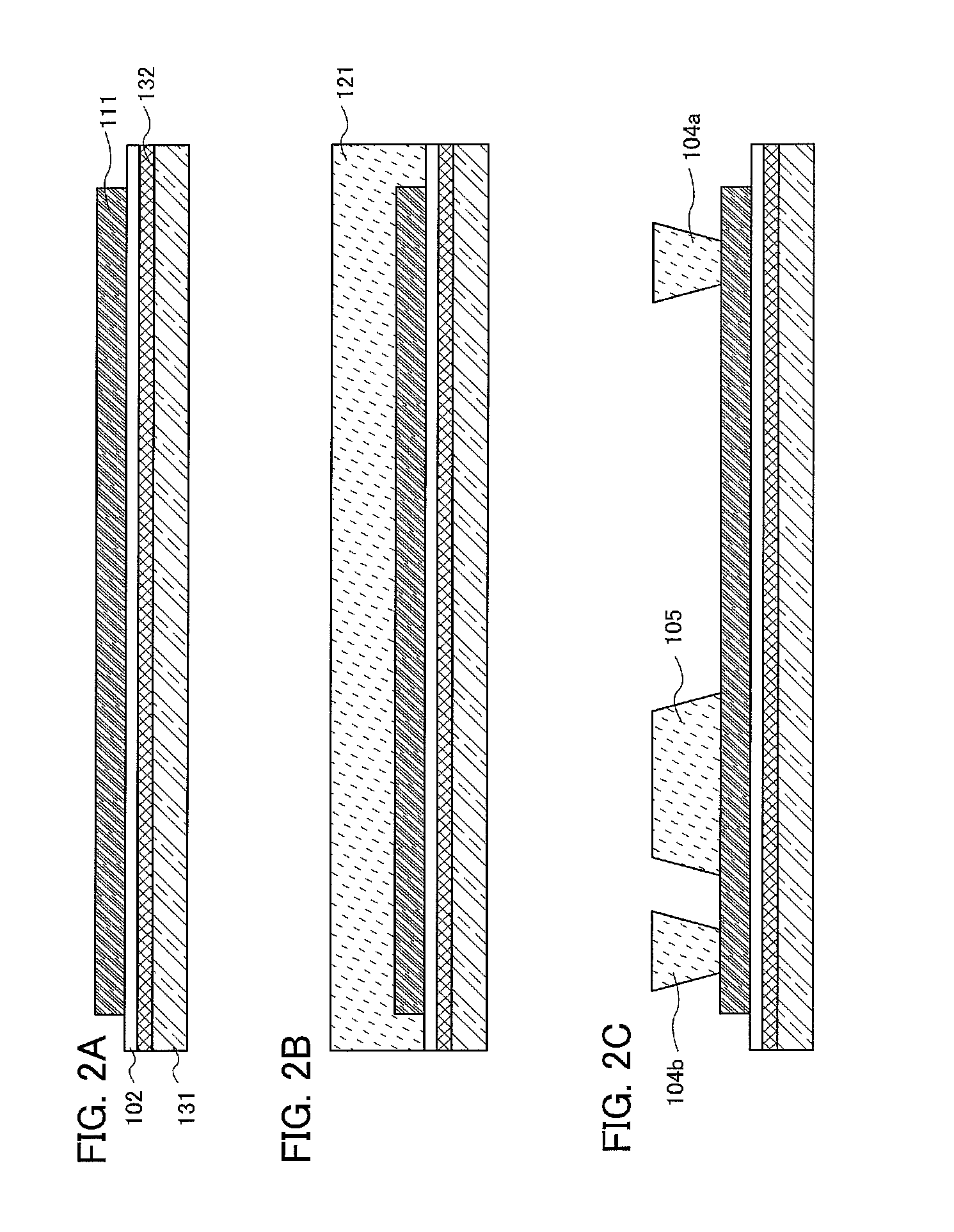
[0062]First, a light-emitting element and a method for manufacturing the light-emitting element are described with reference to FIGS. 2A to 2C, FIGS. 3A and 3B, FIGS. 4A and 4B, FIGS. 5A and 5B, and FIGS. 6A to 6C.

[0063]First, a separation layer 132, a base film 102, and an electrode 111 are formed over a substrate 131 (see FIG. 2A). As the substrate 131, a glass substrate, a quartz substrate, a semiconductor substrate, a ceramic substrate, or the like may be used.

[0064]The base film 102 may be a silicon oxide film, a silicon nitride film, a silicon oxide film containing...

embodiment 2

[0195]In this embodiment, a cellular phone incorporating the light-emitting device described in Embodiment 1 is described with reference to FIGS. 13A to 13D, FIGS. 22A and 22B, FIG. 25, FIG. 26, FIGS. 27A to 27D, and FIGS. 28A and 28B. In this embodiment, the same elements are denoted by the same reference numerals.

[0196]FIG. 13C is a front view of the cellular phone; FIG. 13D, a side view; FIG. 13B, a top view; and FIG. 13A, a cross-sectional view of a housing 411. The shape of the front of the housing 411 is a rectangle having longer sides and shorter sides, which may have round corners. In this embodiment, a direction parallel to the longer sides of the rectangle that is the shape of the front is referred to as a longitudinal direction, and a direction parallel to the shorter sides is referred to as a lateral direction.

[0197]In addition, the shape of the side of the housing 411 is also a rectangle having longer sides and shorter sides, which may have round corners. In this embodi...


PUM


Abstract

The invention relates to: a light-emitting device which includes a first flexible substrate having a first electrode, a light-emitting layer over the first electrode, and a second electrode with a projecting portion over the light-emitting layer and a second flexible substrate having a semiconductor circuit and a third electrode electrically connected to the semiconductor circuit, in which the projecting portion of the second electrode and the third electrode are electrically connected to each other; a method for manufacturing the light-emitting device; and a cellular phone which includes a housing incorporating the light-emitting device and having a longitudinal direction and a lateral direction, in which the light-emitting device is disposed on a front side and in an upper portion in the longitudinal direction of the housing.

Description

BACKGROUND OF THE INVENTION[0001]1. Field of the Invention[0002]The invention disclosed in this specification relates to a light-emitting device, a method for manufacturing the light-emitting device, and a cellular phone.[0003]2. Description of the Related Art[0004]Conventionally, a light-emitting device having a light-emitting element has been formed through the following steps of: 1) forming a semiconductor circuit for driving a light-emitting element over a substrate such as a glass substrate by using a semiconductor process, 2) forming an insulating film (a planarization film) over the semiconductor circuit, and 3) forming a light-emitting element over the insulating film. In other words, a semiconductor circuit for driving a light-emitting element and the light-emitting element are formed by being stacked over a substrate in this order.[0005]Since a light-emitting device manufactured through the conventional manufacturing process has a light-emitting element over a semiconducto...

Claims


Application Information

Patent Timeline
Patent Type & Authority Patents(United States)
IPC IPC(8): H01L33/36H01L51/50
CPCH01L27/3251H01L51/5237H04M1/0268H01L27/3253H01L51/0097H01L2227/323H01L2251/5338Y02E10/549Y02P70/50H04M1/0269H10K59/127H10K59/1275H10K77/111H10K50/846H10K50/841H10K59/1201H10K2102/311H10K59/122H10K59/124H10K71/50
Inventor HATANO, KAORUSEO, SATOSHIYAMAZAKI, SHUNPEI
Owner SEMICON ENERGY LAB CO LTD
Why Eureka
Try Eureka