Semiconductor light emitting device capable of suppressing silver migration of reflection film made of silver

a technology of silver reflection film and semiconductor, applied in the direction of semiconductor device, basic electric element, electrical apparatus, etc., can solve the problem of insufficient migration suppression effect, and achieve the effect of suppressing the ionization of metal constituting the reflection film and suppressing the generation of migration

Active Publication Date: 2006-11-28
STANLEY ELECTRIC CO LTD
View PDF8 Cites 87 Cited by
  • Summary
  • Abstract
  • Description
  • Claims
  • Application Information

AI Technical Summary

Benefits of technology

[0017]An object of this invention is to provide a semiconductor light emitting device capable of suppressing migration and improving reliability although it uses the metal likely to evolve migration.
[0020]The reflection film is connected to the n-side electrode, i.e., cathode. It is therefore possible to suppress ionization of metal constituting the reflection film and suppress the generation of migration.

Problems solved by technology

However, this migration suppression effect is not sufficient.

Method used


Image

  • Semiconductor light emitting device capable of suppressing silver migration of reflection film made of silver
  • Semiconductor light emitting device capable of suppressing silver migration of reflection film made of silver
  • Semiconductor light emitting device capable of suppressing silver migration of reflection film made of silver

Examples


first embodiment

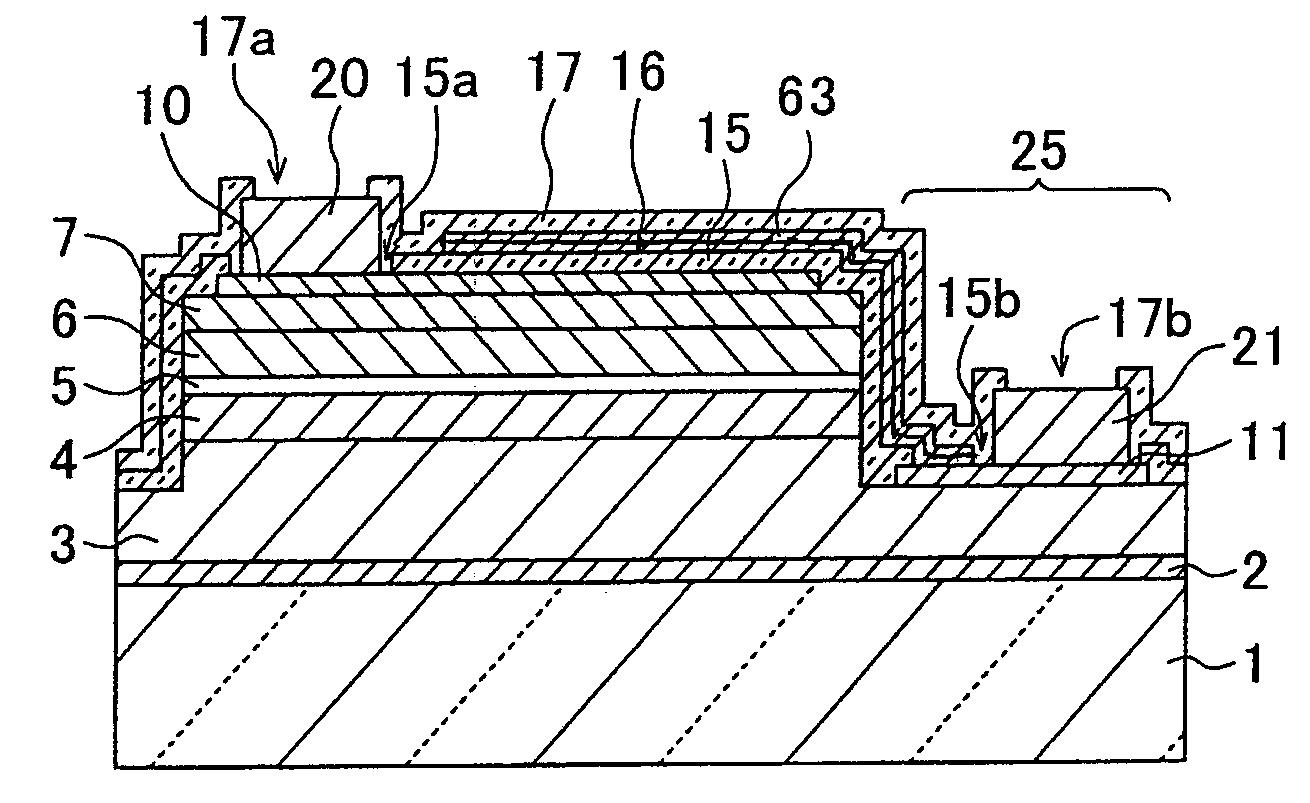
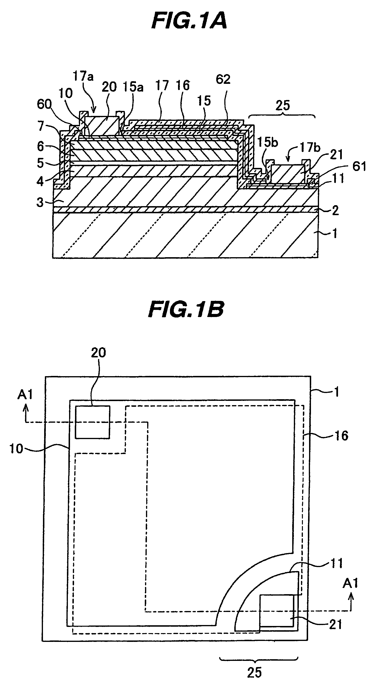
[0041]FIG. 1A is a cross sectional view of a semiconductor light emitting device and FIG. 1B is a plan view of the device shown in FIG. 1A. A cross sectional view taken along one-dot chain line A1—A1 shown in FIG. 1B corresponds to FIG. 1A. On an underlying substrate 1 made of sapphire, an initial nucleus forming layer 2, an n-type contact layer 3, an n-type clad layer 4, a luminous layer 5, a p-type clad layer 6, a p-type contact layer 7 are stacked in this order. These layers are made of nitride compound semiconductor such as InxAlyGazN (x+y+z=1).

[0042]In a first area 25 of a partial substrate in-plane, the layers from the p-type contact layer 7 to a surface layer of the n-type contact layer 3 are etched to partially expose the n-type contact layer 3.

[0043]A p-side ohmic electrode 10 is formed on the p-type contact layer 7. The p-side ohmic electrode 10 is made of platinum (Pt) and has a thickness of about 5 nm. An n-side ohmic electrode 11 is formed on the surface of the n-type ...

second embodiment

[0083]Next, with reference to FIGS. 10 and 11, a semiconductor light emitting device of the second embodiment will be described.

[0084]FIG. 10 is a plan view of a semiconductor light emitting device of the second embodiment. In the first embodiment shown in FIG. 1B, the reflection film 16 is made of a plain film and superposes most area of the p-side ohmic electrode 10. In the second embodiment, in place of the reflection film 16, a reflection pattern 16a of a grid shape is disposed. The other fundamental structure is similar to that of the semiconductor light emitting device of the first embodiment. In the example shown in FIG. 10, although a p-side pad electrode 20 and an n-side pad electrode 21 are disposed slightly inside of the central area of a pair of opposing sides of a rectangle, they may be disposed near at the vertexes of the rectangle as in the case of the first embodiment shown in FIG. 1B.

[0085]In the semiconductor light emitting device of the second embodiment, light ra...

third embodiment

[0091]Next, with reference to FIGS. 12A and 12B and FIG. 13, a semiconductor light emitting device of the third embodiment will be described.

[0092]FIG. 12A is a cross sectional view of the semiconductor light emitting device of the third embodiment, and FIG. 12B is a plan view thereof. A cross sectional view taken along one-dot chain line A12—A12 shown in FIG. 12B corresponds to FIG. 12A. Description will be made on different points from the semiconductor light emitting device of the first embodiment.

[0093]In the first embodiment, the n-side pad electrode 21 is disposed on the n-side ohmic electrode 11, whereas in the second embodiment, an n-side pad electrode 21 is disposed over a p-side ohmic electrode 10 and contacts a reflection film 16. A p-side pad electrode 20 and the n-side pad electrode 21 are exposed on the bottoms of openings 17a and 17b formed through a protective film 17.

[0094]As shown in FIG. 12B, the n-side ohmic electrode 11 is disposed along one side of a support su...


PUM


Abstract

A luminous lamination structure includes a first layer made of n-type nitride semiconductor and a second layer made of p-type nitride semiconductor and disposed over the first layer wherein a luminous region is defined between the first and second layers. The second layer is removed to expose the first layer in a first area which is a partial surface of the first layer. A p-side electrode is disposed on a surface of the second layer and electrically connected to the second layer. An insulating film covers the p-side electrode. An n-side electrode electrically connected to the first layer is disposed in the first area. A reflection film disposed on the insulating film extends to the n-side electrode and electrically connected to the n-side electrode. The reflection film is made of silver containing alloy or silver.

Description

CROSS REFERENCE TO RELATED APPLICATION[0001]This application is based on and claims priority of Japanese Patent Application No. 2004-095217 filed on Mar. 29, 2004, the entire contents of which are incorporated herein by reference.BACKGROUND OF THE INVENTION[0002]A) Field of the Invention[0003]The present invention relates to a semiconductor light emitting device, and more particularly to a semiconductor light emitting device which uses nitride semiconductor and has positive and negative electrodes disposed on the same side of a substrate.[0004]B) Description of the Related Art[0005]FIG. 15A is a cross sectional view of a semiconductor light emitting device disclosed in Japanese Patent Laid-open Publication No. 2003-224297. On a sapphire substrate 200, a buffer layer 201 is formed. On the buffer layer 201, an n-type contact layer 202 of n-type GaN, an n-type clad layer 203 of n-type AlGaN, a light emitting or luminous layer 204 of InGaN, a p-type clad layer 205 of p-type AlGaN and a ...

Claims


Application Information

Patent Timeline
Patent Type & Authority Patents(United States)
IPC IPC(8): H01L27/15H01L29/22H01L33/32H01L33/38H01L33/40H01L33/46H01L33/50
CPCH01L33/46H01L33/40H01L33/32H01L33/38H01L2224/02166H01L2224/0603H01L2224/16145H01L2224/48091H01L2224/48247H01L2224/48257H01L2224/49107H01L2224/8592H01L2224/45144H01L2924/181H01L2924/00014H01L2924/00H01L2924/00012
Inventor HORIO, NAOCHIKATSUCHIYA, MASAHIKOTAMURA, HITOSHI
Owner STANLEY ELECTRIC CO LTD
Why Eureka
Try Eureka