Semiconductor device

a semiconductor and device technology, applied in semiconductor devices, instruments, electrical equipment, etc., can solve the problems of low conductivity of light-transmitting conductive materials such as indium tin oxide, indium zinc oxide, indium tin zinc oxide, and difficulty in supply of normal voltage and normal current, so as to achieve high conductivity, low resistivity, and high conductivity

Active Publication Date: 2010-06-10
SEMICON ENERGY LAB CO LTD
View PDF100 Cites 116 Cited by
  • Summary
  • Abstract
  • Description
  • Claims
  • Application Information

AI Technical Summary

Benefits of technology

[0012]In addition, in terms of display performance, large capacitors and higher aperture ratios are demanded for pixels. Pixels each having a high aperture ratio increase the use efficiency of light, so that power saving and miniaturization of a display device can be achieved. In recent years, the size of pixels has been miniaturized and images with higher definition are demanded. The miniaturization of the size of pixels causes a decrease in the aperture ratio of the pixel because of the large formation area for transistors and wirings which occupies one pixel. Accordingly, in order to obtain a high aperture ratio in each pixel in a regulation size, it is necessary to efficiently lay out circuit components needed for the circuit configuration of the pixel.
[0013]In view of the foregoing problems, an object is to provide a semiconductor device with high aperture ratio and a manufacturing method thereof. In addition, an object is to provide a semiconductor device with low power consumption and a manufacturing method thereof.
[0020]Further, in the above, by using a multi-tone mask, a light-transmitting region (a region with high light transmissivity) and a light-blocking region (a region with low light transmissivity) can be formed with one mask (reticle). Accordingly, the light-transmitting region (the region with high light transmissivity) and the light-blocking region (the region with low light transmissivity) can be formed without increasing the number of masks.
[0023]According to an embodiment of the invention disclosed, a light-transmitting transistor or a light-transmitting capacitor can be formed. Therefore, even if a transistor or a capacitor is provided in a pixel, the aperture ratio can be high because light can be transmitted also in a portion where the transistor or the capacitor is formed. Further, since a wiring for connecting the transistor and an element (e.g., another transistor) or a wiring for connecting a capacitor and an element (e.g., another capacitor) can be formed using a material with low resistivity and high conductivity, the distortion of the waveform of a signal and a voltage drop due to wiring resistance can be reduced.

Problems solved by technology

However, in general, as compared to a material having a light-blocking property and a reflecting property, such as aluminum, molybdenum, titanium, tungsten, neodymium, copper, or silver, a light-transmitting conductive material such as indium tin oxide, indium zinc oxide, or indium tin zinc oxide has low conductivity.
As wiring resistance increases, the waveform of a signal which is transmitted through the wiring becomes distorted, and a voltage drop due to the wiring resistance results in a low voltage supply.
Therefore, it is difficult to supply a normal voltage and a normal current, whereby normal display and operation are difficult.

Method used


Image

  • Semiconductor device
  • Semiconductor device
  • Semiconductor device

Examples


embodiment 1

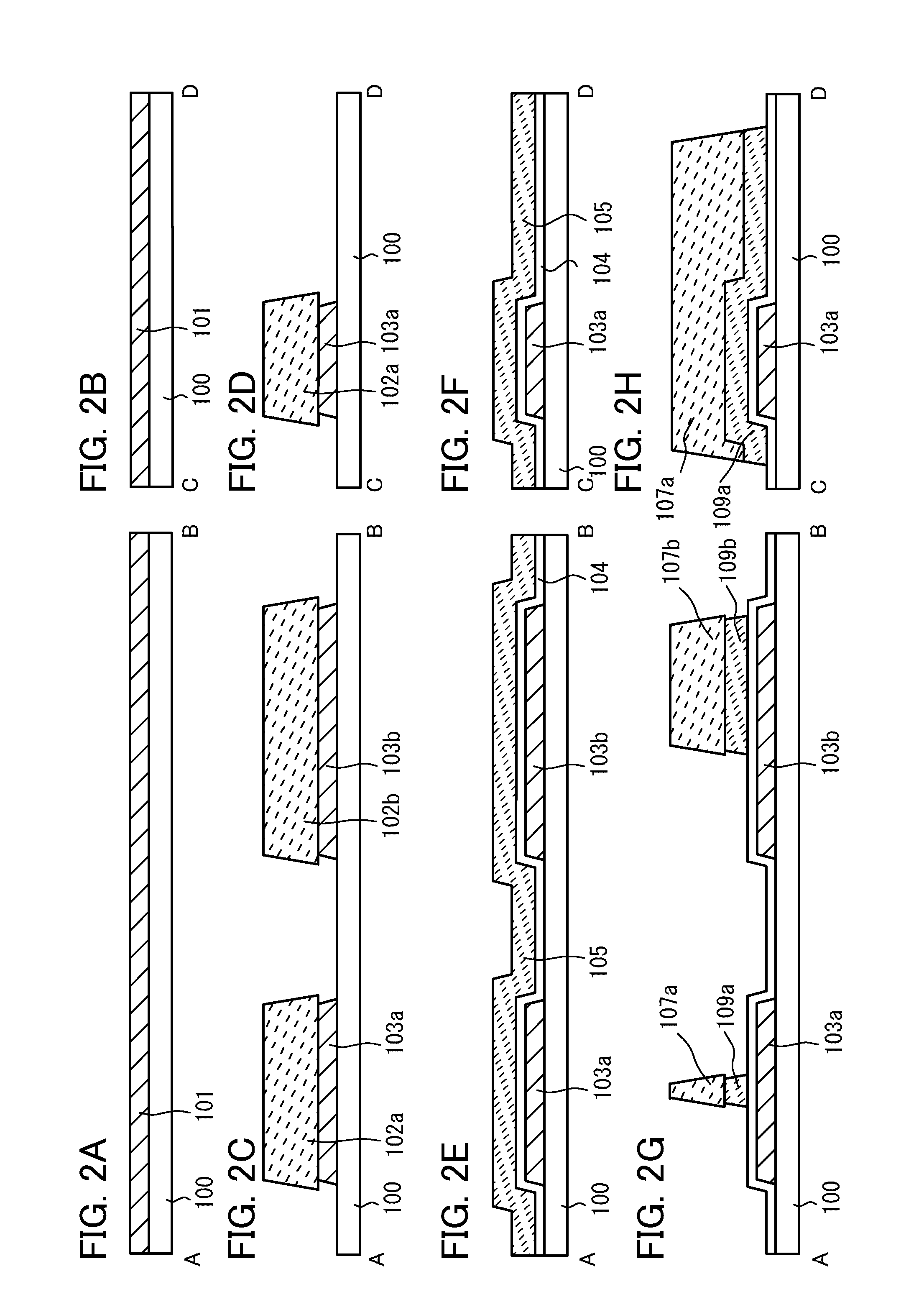
[0059]In this embodiment, a semiconductor device and a manufacturing process thereof will be described with reference to FIGS. 1A and 1B, FIGS. 2A to 2H, FIGS. 3A to 3H, FIGS. 4A to 4F, FIGS. 5A to 5F, FIG. 6, FIGS. 7A to 7C, FIGS. 8A to 8C, FIG. 9, FIGS. 10A and 10B, FIGS. 11A and 11B, and FIG. 12.

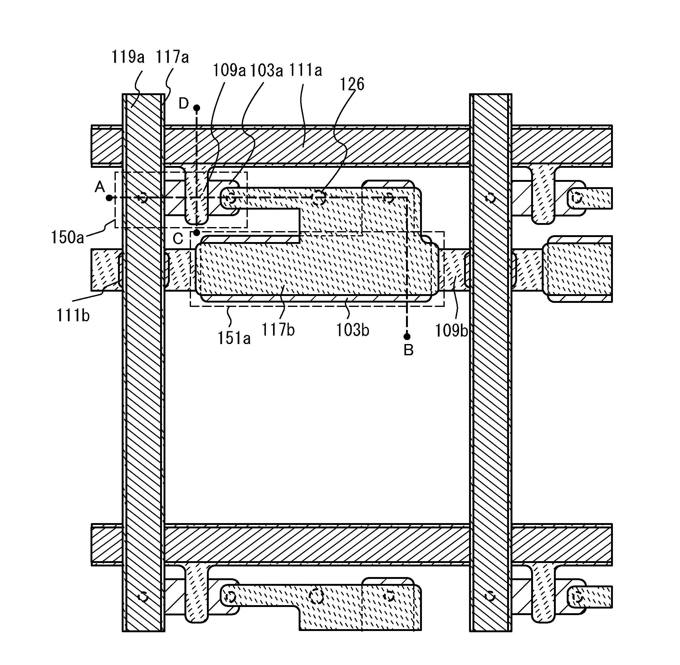
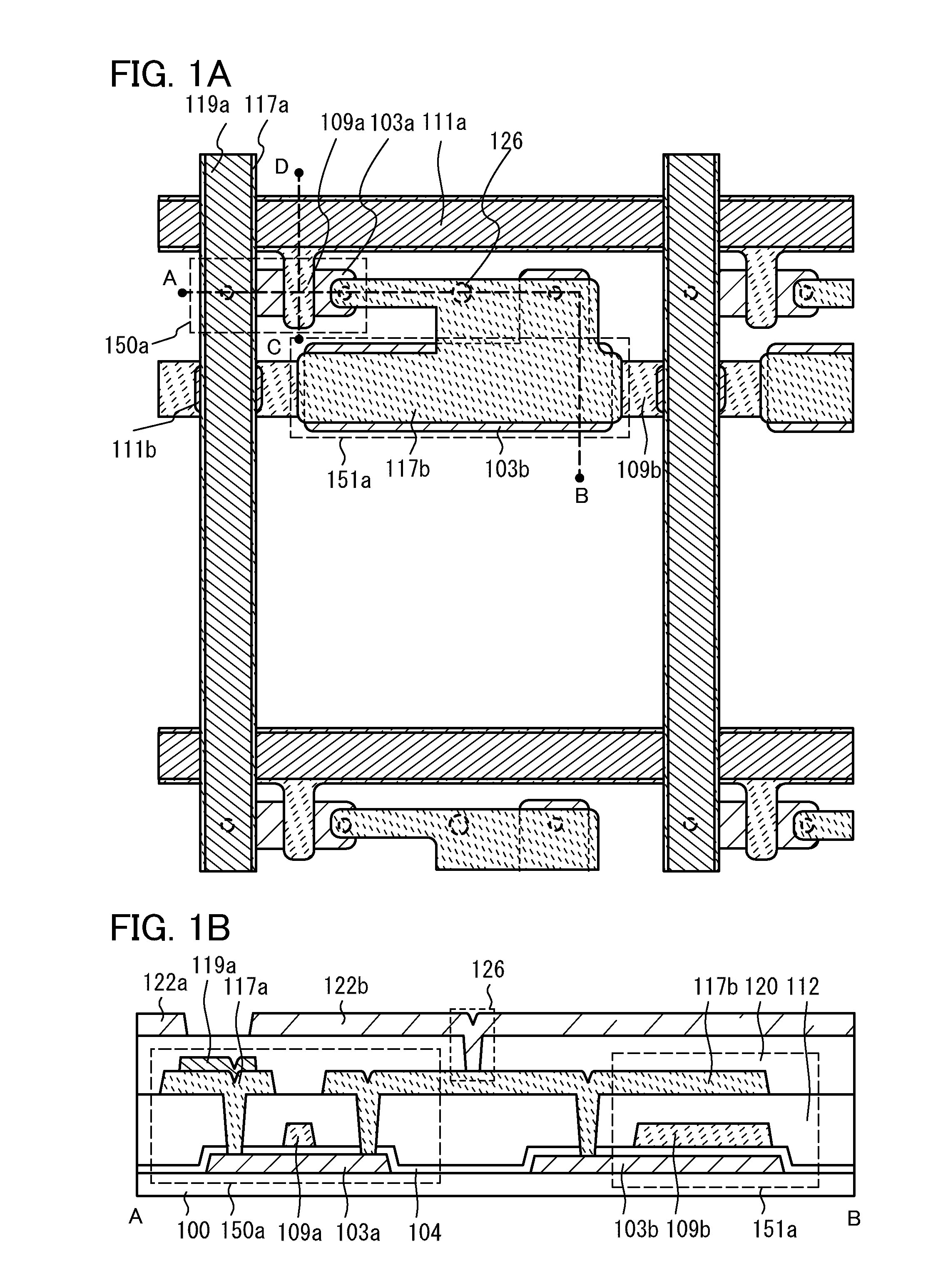
[0060]FIGS. 1A and 1B illustrate a semiconductor device according to this embodiment. FIG. 1A is a top view and FIG. 1B is a cross-sectional view taken along line A-B of FIG. 1A.

[0061]A semiconductor device illustrated in FIG. 1A includes a pixel portion which has a gate wiring and a capacitor wiring provided in a direction 1, a source wiring provided in a direction 2, which intersects with the gate wiring and the capacitor wiring, and a transistor 150a in the vicinity of an intersection of the gate wiring and the source wiring. Note that in this specification, the pixel portion refers to a region surrounded by a plurality of gate wirings and a plurality of source wirings.

[0062]The transi...

embodiment 2

[0137]In this embodiment, an example of a manufacturing process of a semiconductor device will be described with reference to FIGS. 13A and 13B, 14A to 14F, 15A to 15D, 16A to 16D, 17A to 17D, 18A to 18D, 19A1 to 19B2, 20A and 20B, 21A and 21B, and 22A and 22B. Note that many portions are common to a semiconductor device according to this embodiment and a manufacturing process thereof and the semiconductor device according to Embodiment 1 and the manufacturing process thereof. Therefore, description of common portions is omitted and different points will be described in detail.

[0138]FIGS. 13A and 13B illustrate the semiconductor device of this embodiment. FIG. 13A is a plan view and FIG. 13B is a cross-sectional view taken along line A-B of FIG. 13A.

[0139]FIGS. 13A and 13B are different from FIGS. 1A and 1B as follows. In FIGS. 1A and 1B, the oxide semiconductor layer 103a and the oxide semiconductor layer 103b are formed for the transistor 150a and the storage capacitor portion 151...

embodiment 3

[0182]In this embodiment, an example will be described in which at least part of a driver circuit and a thin film transistor provided in a pixel portion are formed over one substrate.

[0183]FIG. 21A is an example of a block diagram of an active matrix liquid crystal display device which is an example of display devices. The display device illustrated in FIG. 21A includes, over a substrate 5300, a pixel portion 5301 which includes a plurality of pixels each provided with a display element, a scan line driver circuit 5302 which selects a pixel, and a signal line driver circuit 5303 which controls input of a video signal to the selected pixel.

[0184]A light-emitting display device illustrated in FIG. 21B includes, over a substrate 5400, a pixel portion 5401 which includes a plurality of pixels each provided with a display element, a first scan line driver circuit 5402 which selects a pixel, a second scan line driver circuit 5404 which selects a pixel, and a signal line driver circuit 540...


PUM


Abstract

A semiconductor device includes an oxide semiconductor layer provided over a substrate having an insulating surface; a gate insulating film covering the oxide semiconductor layer; a first conductive layer and a second conductive layer laminated in this order over the gate insulating film; an insulating film covering the oxide semiconductor layer and a gate wiring including a gate electrode (the first and second conductive layers); and a third conductive layer and a fourth conductive layer laminated in this order over the insulating film and electrically connected to the oxide semiconductor layer. The gate electrode is formed using the first conductive layer. The gate wiring is formed using the first conductive layer and the second conductive layer. A source electrode is formed using the third conductive layer. A source wiring is formed using the third conductive layer and the fourth conductive layer.

Description

BACKGROUND OF THE INVENTION[0001]1. Field of the Invention[0002]The present invention relates to a semiconductor device provided with a circuit including a thin film transistor (hereinafter referred to as a TFT) using an oxide semiconductor film for a channel formation region and a method for manufacturing the semiconductor device. For example, the present invention relates to an electronic appliance having as a component an electro-optical device typified by a liquid crystal display panel or a light-emitting display device including an organic light-emitting element.[0003]2. Description of the Related Art[0004]As typically seen in a liquid crystal display device, a thin film transistor formed over a flat plate such as a glass substrate is manufactured using amorphous silicon or polycrystalline silicon. A thin film transistor manufactured using amorphous silicon has low field effect mobility, but can be formed over a large glass substrate. In contrast, a thin film transistor manufac...

Claims


Application Information

Patent Timeline
Patent Type & Authority Applications(United States)
IPC IPC(8): H01L29/22
CPCH01L27/1225H01L27/1288H01L27/124H01L27/1255H01L29/66969G02F1/133345G02F1/133528G02F1/13439G02F1/136277G02F1/136286G02F1/1368G02F2201/40H01L29/7869H01L27/1214H01L27/13H01L29/45
Inventor KIMURA, HAJIME
Owner SEMICON ENERGY LAB CO LTD
Why Eureka
Try Eureka