Semiconductor device and manufacturing method thereof

a semiconductor and manufacturing method technology, applied in static indicating devices, instruments, optics, etc., can solve the problems of increasing the power consumption of the semiconductor device, and achieve the effects of high reliability of the semiconductor device, and low power consumption

Active Publication Date: 2011-09-08
SEMICON ENERGY LAB CO LTD
View PDF102 Cites 85 Cited by
  • Summary
  • Abstract
  • Description
  • Claims
  • Application Information

AI Technical Summary

Benefits of technology

[0026]An embodiment of the present invention can provide a highly reliable semiconductor device. Further, another embodiment of the present invention can provide a manufacturing method of a highly reliable semiconductor device.
[0027]An embodiment of the present invention can provide a semiconductor device having low power consumption. Further, another embodiment of the present invention can provide a manufacturing method of a semiconductor device having low power consumption.
[0028]An embodiment of the present invention can provide a semiconductor device which can be manufactured with high mass productivity. Further, an embodiment of the present invention can provide a manufacturing method of a semiconductor device which can be manufactured with high mass productivity.

Problems solved by technology

Further, if a transistor having a large off-state current is used in a semiconductor device, power consumption of the semiconductor device is increased.

Method used


Image

  • Semiconductor device and manufacturing method thereof
  • Semiconductor device and manufacturing method thereof
  • Semiconductor device and manufacturing method thereof

Examples


embodiment 1

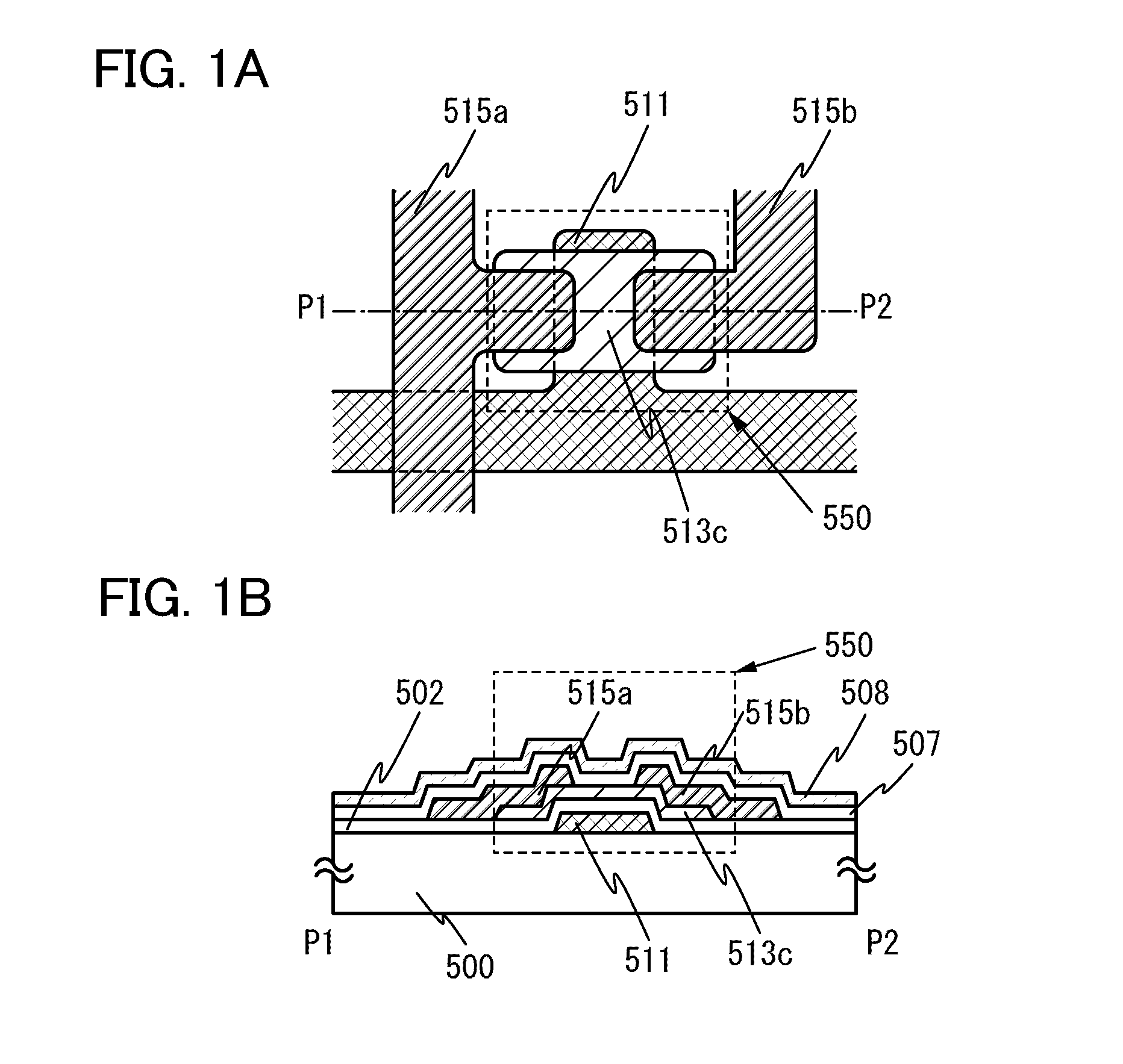
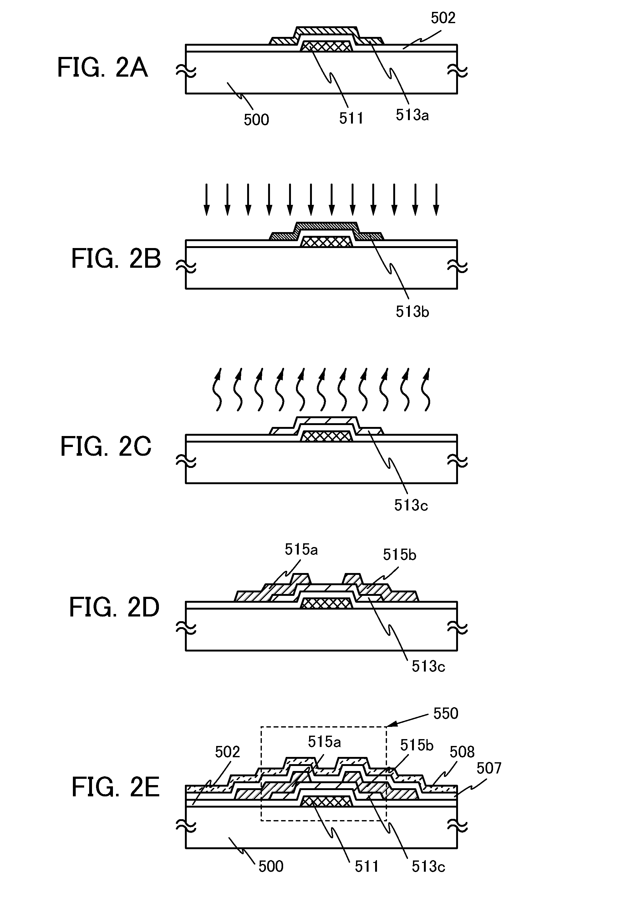
[0053]In this embodiment, a manufacturing method of a bottom-gate transistor using a method for purifying an oxide semiconductor layer by adding fluorine into an oxide semiconductor layer and then subjecting the oxide semiconductor layer to heat treatment to remove impurities will be described with reference to FIGS. 1A and 1B and FIGS. 2A to 2E.

[0054]FIGS. 1A and 1B illustrate a structure of a bottom-gate transistor 550 which is manufactured in this embodiment. FIG. 1A is a top view of the transistor 550, and FIG. 1B is a cross-sectional view of the transistor 550. Note that FIG. 1B corresponds to the cross-sectional view taken along line P1-P2 in FIG. 1A.

[0055]In the transistor 550, a gate electrode 511 and a gate insulating layer 502 which covers the gate electrode 511 are provided over a substrate 500 having an insulating surface. A purified oxide semiconductor layer 513c which overlaps with the gate electrode 511 is provided over the gate insulating layer 502. In addition, a fi...

embodiment 2

[0149]In this embodiment, a manufacturing method of a top-gate transistor using a method for purifying an oxide semiconductor layer by adding fluorine into an oxide semiconductor layer and then subjecting the oxide semiconductor layer to heat treatment to remove impurities will be described with reference to FIGS. 3A and 3B and FIGS. 4A to 4E.

[0150]FIGS. 3A and 3B illustrate a structure of a top-gate transistor 650 which is manufactured in this embodiment. FIG. 3A is a top view of the transistor 650, and FIG. 3B is a cross-sectional view of the transistor 650. Note that FIG. 3B corresponds to the cross-sectional view taken along line Q1-Q2 in FIG. 3A.

[0151]In the transistor 650, over a substrate 600 having an insulating surface, a first electrode 615a and a second electrode 615b which each function as a source or drain electrode are provided. A purified oxide semiconductor layer 613c which covers end portions of the first electrode 615a and the second electrode 615b, and a gate insu...

embodiment 3

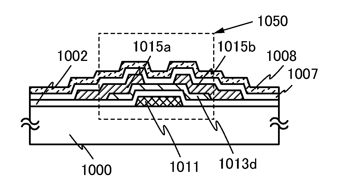
[0184]In this embodiment, a manufacturing method of a bottom-gate transistor using a method for purifying an oxide semiconductor layer, which is different from the method of Embodiment 1, by adding fluorine into an oxide semiconductor layer and then subjecting the oxide semiconductor layer to heat treatment to remove impurities will be described with reference to FIGS. 10A and 10B, FIGS. 11A to 11C, and FIGS. 12A to 12C.

[0185]FIGS. 10A and 10B illustrate a structure of a bottom-gate transistor 1050 which is manufactured in this embodiment. FIG. 10A is a top view of the transistor 1050, and FIG. 10B is a cross-sectional view of the transistor 1050. Note that FIG. 10B corresponds to the cross-sectional view taken along line R1-R2 in FIG. 10A.

[0186]In the transistor 1050, a gate electrode 1011 and a gate insulating layer 1002 which covers the gate electrode 1011 are provided over a substrate 1000 having an insulating surface. A purified oxide semiconductor layer 1013d which overlaps wi...


PUM


Abstract

An object of the present invention to provide a highly reliable semiconductor device. Another object is to provide a manufacturing method of a highly reliable semiconductor device. Still another object is to provide a semiconductor device having low power consumption. Yet another object is to provide a manufacturing method of a semiconductor device having low power consumption. Furthermore, another object is to provide a semiconductor device which can be manufactured with high mass productivity. Another object is to provide a manufacturing method of a semiconductor device which can be manufactured with high mass productivity. An impurity remaining in an oxide semiconductor layer is removed so that the oxide semiconductor layer is purified to have an extremely high purity. Specifically, after adding a halogen element into the oxide semiconductor layer, heat treatment is performed to remove an impurity from the oxide semiconductor layer. The halogen element is preferably fluorine.

Description

TECHNICAL FIELD[0001]The present invention relates to a semiconductor device including an oxide semiconductor. The present invention also relates to a manufacturing method of the semiconductor device. Note that semiconductor devices herein refer to general elements and devices which function by utilizing semiconductor characteristics.BACKGROUND ART[0002]A technique in which a transistor is formed using a semiconductor layer formed over a substrate having an insulating surface is known. For example, a technique in which a transistor is formed over a glass substrate using a thin film including a silicon-based semiconductor material and the transistor is applied to a liquid crystal display device or the like is known.[0003]A transistor which is used in a liquid crystal display device is generally formed using a semiconductor material such as amorphous silicon or polycrystalline silicon. Although transistors including amorphous silicon have low field effect mobility, a larger glass subs...

Claims


Application Information

Patent Timeline
Patent Type & Authority Applications(United States)
IPC IPC(8): H01L29/786H01L21/44
CPCH01L21/02554H01L21/02565H01L21/02573H01L21/02614H01L21/02631H01L21/02667G02F1/1368H01L27/11521H01L27/1156H01L27/1203H01L27/1225H01L29/7869H01L21/3228H10B41/30H10B41/70H01L21/324H01L29/66742H10B99/00G02F1/133345G02F1/134309G02F1/13439G02F1/137G02F2201/121G02F2201/123G09G3/3648G09G2310/08G09G2330/021G11C16/10G11C16/14G11C16/26H01L21/477H01L29/247H01L29/66969H01L29/78693H01L29/78696
Inventor YAMAZAKI, SHUNPEIKISHIDA, HIDEYUKI
Owner SEMICON ENERGY LAB CO LTD
Why Eureka
Try Eureka