Semiconductor device and manufacturing method thereof

a semiconductor device and manufacturing method technology, applied in the field of semiconductor devices, can solve the problems of increasing the power consumption of the semiconductor device, reducing the time of use, and shortening the traveling distance of the in-vehicle electronic device, so as to reduce the concentration of hydrogen, reduce the leakage current, and reduce the effect of power consumption

Active Publication Date: 2013-04-16
SEMICON ENERGY LAB CO LTD
View PDF150 Cites 83 Cited by
  • Summary
  • Abstract
  • Description
  • Claims
  • Application Information

AI Technical Summary

Benefits of technology

[0010]Power consumption of electronic devices in a standby period is regarded as important in addition to power consumption in an operating period. Specifically, as for portable electronic devices, to which power is supplied from battery, time of use is limited due to limited amount of electric power. Further, as for in-vehicle electronic devices, when leakage current in a standby period is large, lifetime of battery may be reduced. In the case of an electric vehicle, leakage current of the in-vehicle electronic device shortens the traveling distance per a certain amount of charging.
[0011]In order to reduce power consumption, reducing leakage current in a standby period in addition to power consumption in an operating period is effective. Although the amount of leakage current of each transistor is not large, several millions of transistors are provided in the LSI, and when the amount of leakage current of those transistors is added up, the resulting amount is by no means small. Such leakage current causes an increase in power consumption of the semiconductor device in a standby period. Although leakage current is caused by various factors, electric power can be saved in a driver circuit or the like which is used in electronic devices, if leakage current in a standby period can be reduced.
[0012]Therefore, an object of the present invention is to reduce leakage current of a transistor used for an LSI, a CPU, or a memory.

Problems solved by technology

Specifically, as for portable electronic devices, to which power is supplied from battery, time of use is limited due to limited amount of electric power.
In the case of an electric vehicle, leakage current of the in-vehicle electronic device shortens the traveling distance per a certain amount of charging.
Such leakage current causes an increase in power consumption of the semiconductor device in a standby period.

Method used


Image

  • Semiconductor device and manufacturing method thereof
  • Semiconductor device and manufacturing method thereof
  • Semiconductor device and manufacturing method thereof

Examples


embodiment 1

[0050]This embodiment describes an example of a cross-sectional structure of a semiconductor integrated circuit.

[0051]In this embodiment, one embodiment of a semiconductor integrated circuit and a manufacturing method thereof is described with reference to FIGS. 1A and 1B, FIG. 2, FIG. 3, and FIGS. 4A and 4B.

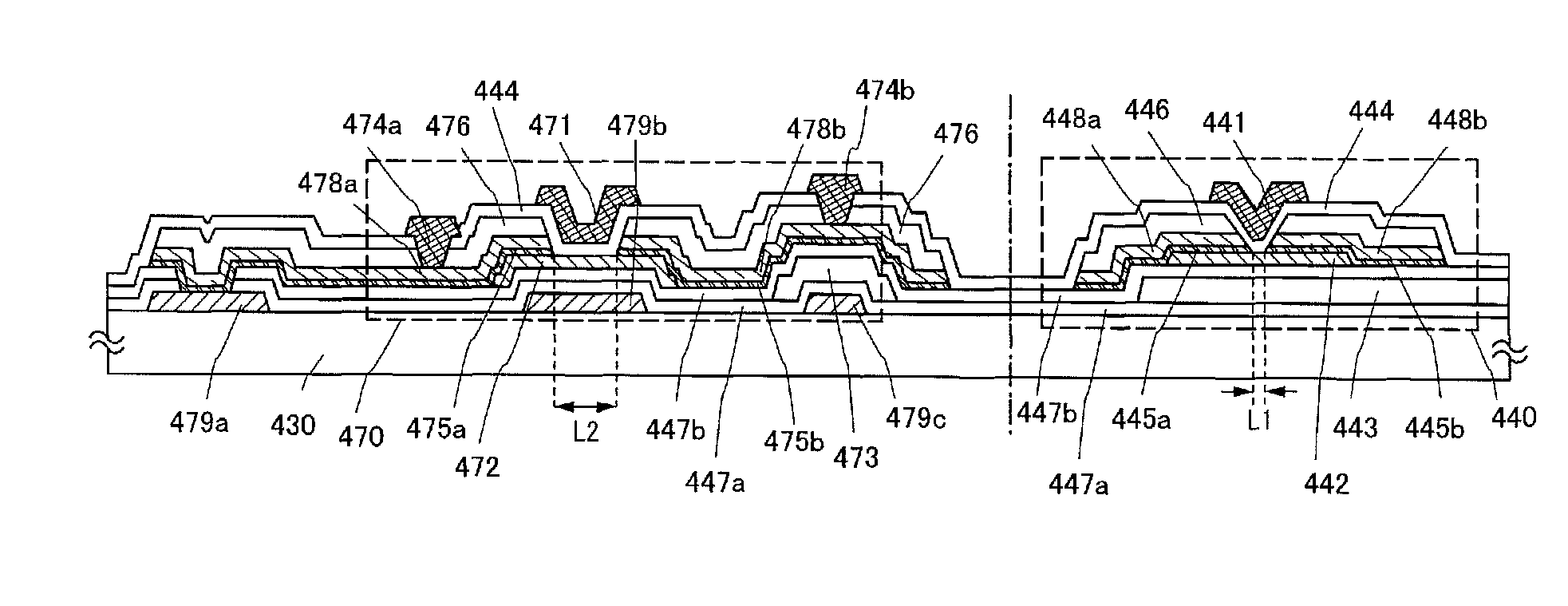
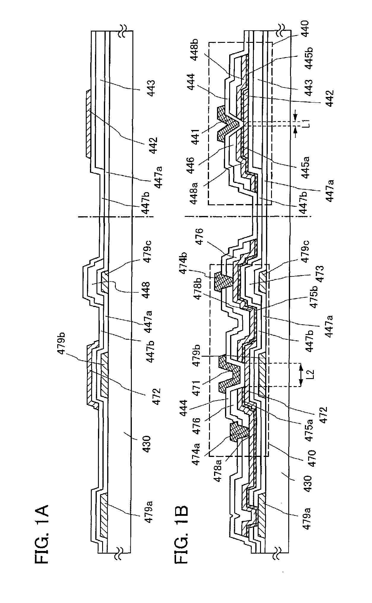
[0052]An example of a cross-sectional structure of the semiconductor integrated circuit is illustrated in FIGS. 1A and 1B. A thin film transistor 440 illustrated in FIG. 1B is one of top-gate thin film transistors.

[0053]The thin film transistor 440 includes a first insulating layer 447a, a second insulating layer 443, a third insulating layer 447b, an oxide semiconductor layer 442, a first source electrode layer 445a, a second source electrode layer 448a, a first drain electrode layer 445b, a second drain electrode layer 448b, a gate insulating layer 444, and a gate electrode layer 441, over a substrate 430 having an insulating surface.

[0054]Part of the oxide semiconductor layer...

embodiment 2

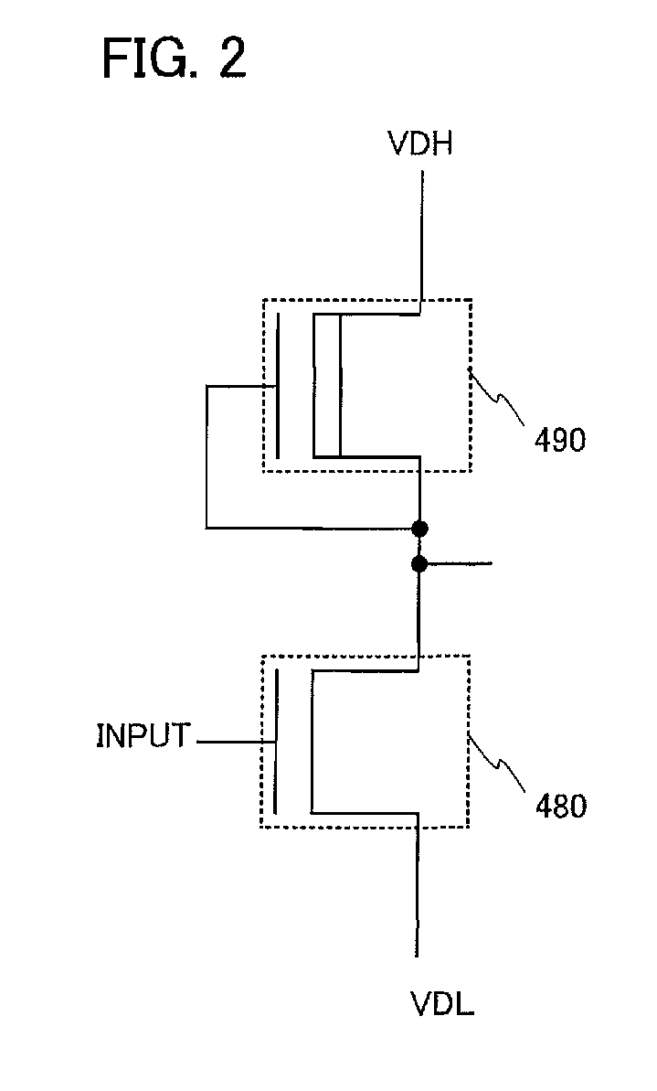
[0131]In Embodiment 1, the thin film transistor 470 including a wiring intersection and the thin film transistor 440 including the gate electrode layer 441 only above the oxide semiconductor layer 442 is described. Hereinafter, an example of forming an inverter circuit of an integrated circuit using two n-channel thin film transistors will be described. Note that since the manufacturing process of the thin film transistor is almost the same as that in Embodiment 1, only different points are described in detail.

[0132]An integrated circuit is formed using an inverter circuit, a capacitor, a resistor, and the like; therefore, a process of forming a capacitor and two kinds of resistors over one substrate in addition to the inverter circuit is also described.

[0133]When the inverter circuit is formed using two n-channel TFTs in combination, there are two kinds of inverter circuits: an inverter circuit having a combination of an enhancement type transistor and a depletion type transistor (...

embodiment 3

[0156]In this embodiment, an example of manufacturing a CPU (central processing unit) using the EDMOS circuit described in Embodiment 2 will be described.

[0157]An example of a block diagram of a CPU is illustrated in FIG. 5. A CPU 1001 illustrated in FIG. 5 includes a timing control circuit 1002, an instruction decoder 1003, a register array 1004, an address logic and buffer circuit 1005, a data bus interface 1006, an ALU 1007, an instruction register 1008, and the like.

[0158]These circuits are manufactured using the thin film transistor, the inverter circuit, the resistor, the capacitor, and the like described in Embodiment 1 or Embodiment 2. The thin film transistors described in Embodiment 1 or Embodiment 2 each use an oxide semiconductor layer with sufficiently reduced hydrogen concentration, whereby the off-current of the thin film transistor can be extremely small. By using a thin film transistor including an oxide semiconductor layer with sufficiently reduced hydrogen concent...


PUM


Abstract

An object is to reduce leakage current and parasitic capacitance of a transistor used for an LSI, a CPU, or a memory. A semiconductor integrated circuit such as an LSI, a CPU, or a memory is manufactured using a thin film transistor in which a channel formation region is formed using an oxide semiconductor which becomes an intrinsic or substantially intrinsic semiconductor by removing impurities which serve as electron donors (donors) from the oxide semiconductor and has larger energy gap than that of a silicon semiconductor. With use of a thin film transistor using a highly purified oxide semiconductor layer with sufficiently reduced hydrogen concentration, a semiconductor device with low power consumption due to leakage current can be realized.

Description

TECHNICAL FIELD[0001]The present invention relates to a semiconductor device including an integrated circuit which includes a thin film transistor (hereinafter, referred to as a TFT) and a manufacturing method thereof. For example, the present invention relates to an electronic device on which a semiconductor integrated circuit is mounted as a component.[0002]In this specification, a “semiconductor device” generally refers to a device which can function by utilizing semiconductor characteristics; an electro-optical device, a semiconductor circuit, an electronic component, and an electronic device are all included in semiconductor devices.BACKGROUND ART[0003]In recent years, semiconductor devices have been developed to be used as an LSI, a CPU, or a memory. A CPU is an aggregation of semiconductor elements each provided with an electrode which is a connection terminal, which includes a semiconductor integrated circuit (including at least a transistor and a memory) separated from a se...

Claims


Application Information

Patent Timeline
Patent Type & Authority Patents(United States)
IPC IPC(8): H01L29/10H01L31/12H01L33/00H01L29/12H01L29/26H01L27/15H01L31/00H01L29/04
CPCH01L27/1225H01L29/26H01L29/7869H01L29/06G06K19/07758G11C7/00G11C19/28H01L21/8236H01L23/66H01L27/0883H01L29/24H01L29/66969H01L29/78609H01L29/78696H01L2223/6677H02M3/07
Inventor YAMAZAKI, SHUNPEIKOYAMA, JUNMIYAKE, HIROYUKITAKAHASHI, KEITOYOTAKA, KOUHEITSUBUKU, MASASHINODA, KOSEIKUWABARA, HIDEAKI
Owner SEMICON ENERGY LAB CO LTD
Why Eureka
Try Eureka