

Semiconductor device including spiral data path
a technology of semiconductor devices and data paths, applied in semiconductor devices, digital storage, instruments, etc., can solve the problem of reducing and achieve the effect of increasing the timing margin of data transfer and significantly reducing the signal path parametric capacity
- Summary
- Abstract
- Description
- Claims
- Application Information
AI Technical Summary
Benefits of technology
Problems solved by technology
Method used
Image

Examples
Embodiment Construction
[0044]Hereinafter, embodiments of the present invention will be described in detail with reference to accompanying drawings.
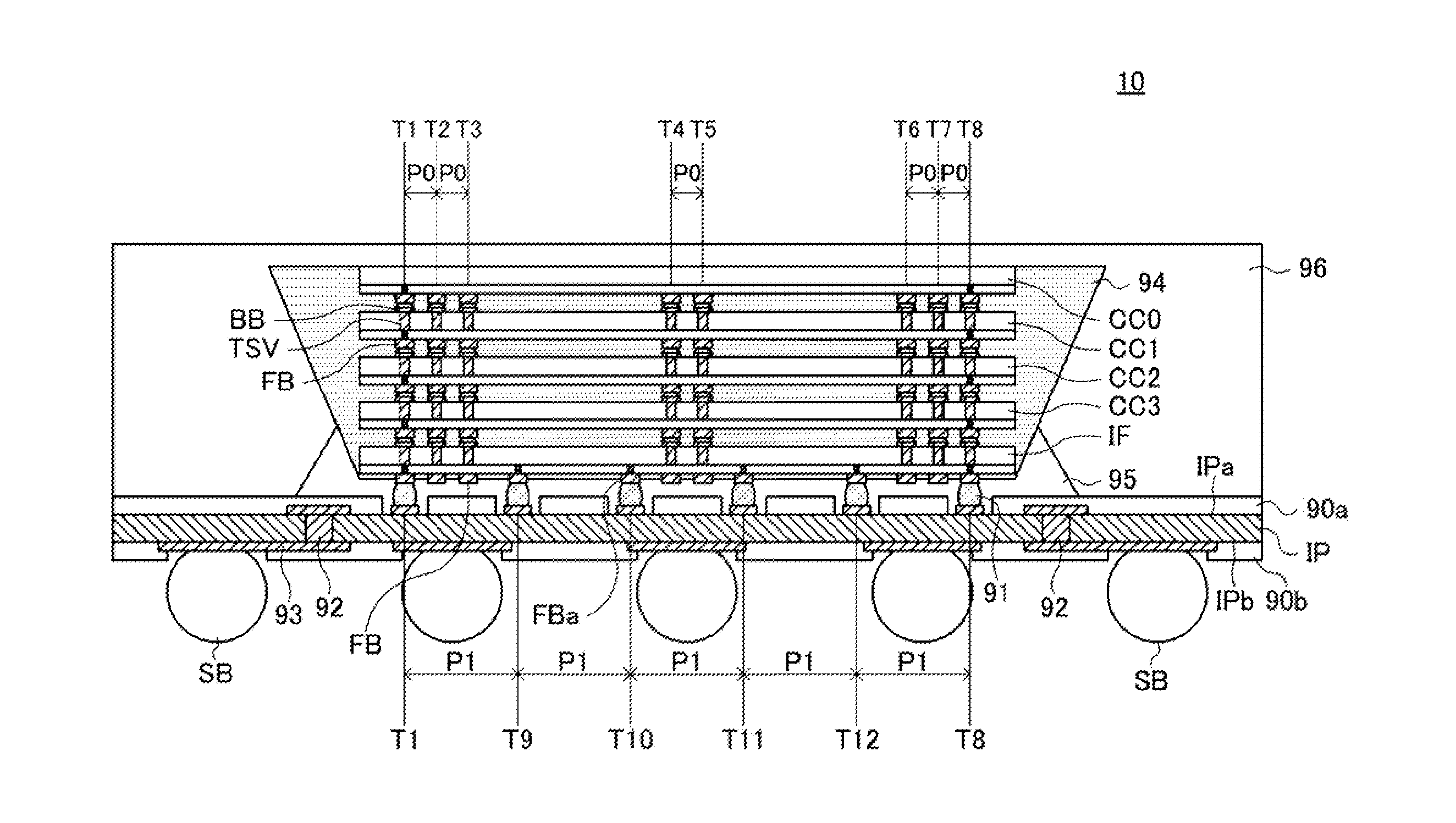
[0045]FIG. 1 is a schematic cross-sectional view illustrating the structure of a semiconductor device 10 according to an embodiment of the present invention.
[0046]As shown in FIG. 1, the semiconductor device 10 according to the present embodiment has a structure in which four core chips CC0 to CC3 having mutually identical functions and may be fabricated using identical manufacturing masks, a single interface chip IF fabricated by using a manufacturing mask different from that for the core chips CC0 to CC3, and a single interposer IP are stacked. The core chips CC0 to CC3 and the interface chip IF are semiconductor chips using silicon substrates and are stacked on the interposer IP in a face-down method. The face-down method means a method in which a semiconductor chip is mounted so that a principal surface on which circuit elements such as transistors are form...
PUM
 Abstract
Description
Claims
Application Information