Display apparatus with active matrix display panel, and method for driving same

a display panel and display apparatus technology, applied in the direction of instruments, static indicating devices, etc., can solve the problems of degrading display quality, increasing the driving voltage, and increasing the power consumption, so as to prevent a degradation of display quality and suppress gate stress

Inactive Publication Date: 2007-04-12
PIONEER CORP
View PDF5 Cites 192 Cited by
  • Summary
  • Abstract
  • Description
  • Claims
  • Application Information

AI Technical Summary

Benefits of technology

[0004] It is an object of the present invention to provide a display apparatus with an active matrix display panel which

Problems solved by technology

In a conventional driving method, since a driving voltage and driving conditions must be set in consideration of variations in Vth due to the gate stress in addition to variations in the initial value of Vth, the driving voltage is inc

Method used


Image

  • Display apparatus with active matrix display panel, and method for driving same
  • Display apparatus with active matrix display panel, and method for driving same
  • Display apparatus with active matrix display panel, and method for driving same

Examples


Embodiment Construction

[0021] In the following, embodiments of the present invention will be described in detail with reference to the drawings.

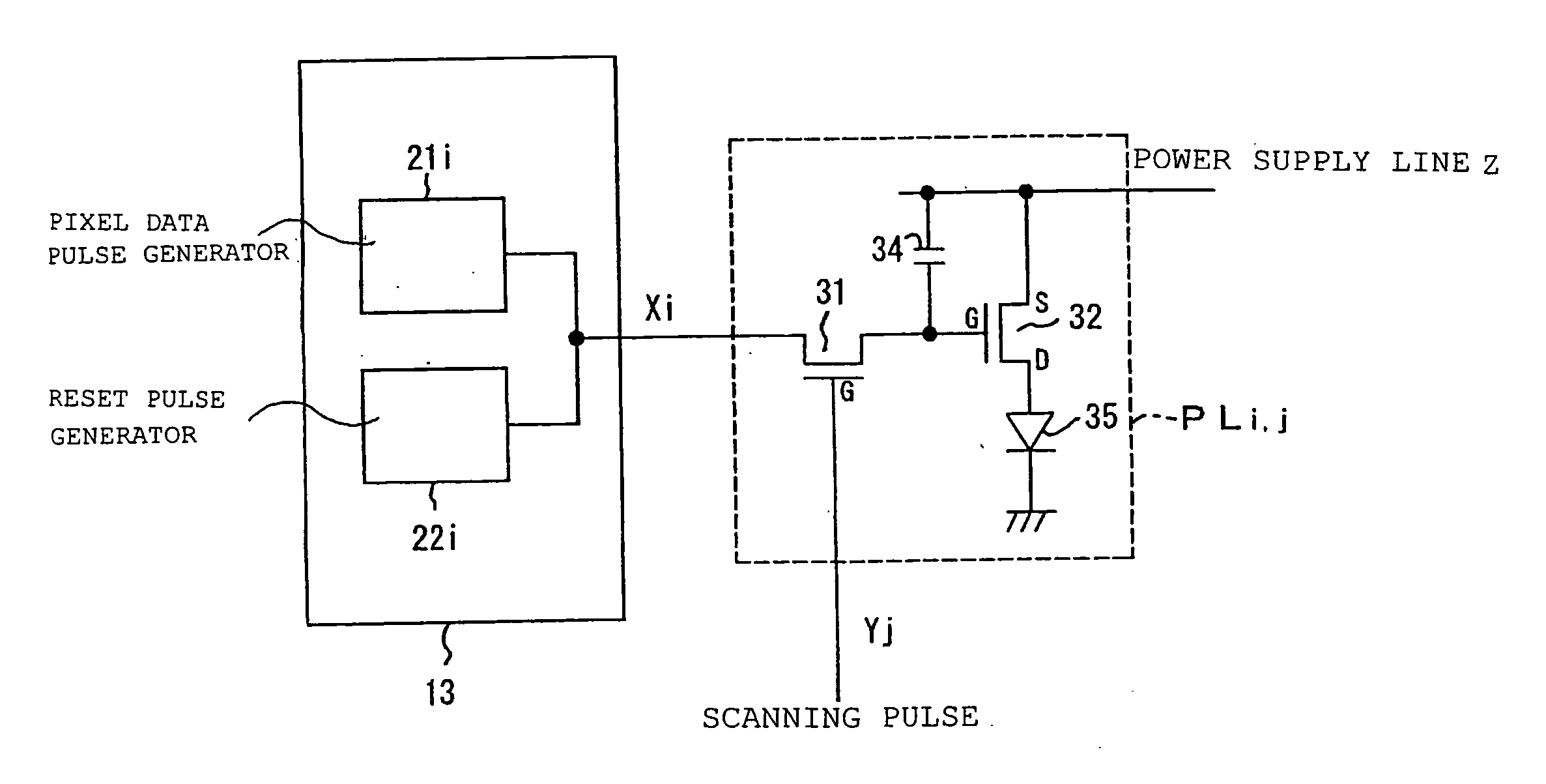
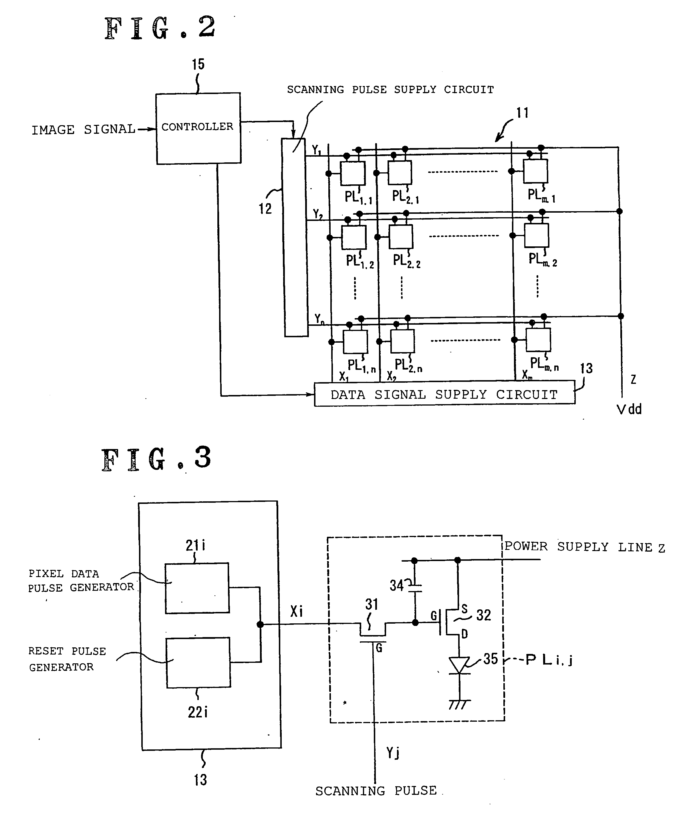
[0022]FIG. 2 shows a display apparatus with an active matrix display panel according to the present invention. The display apparatus comprises a display panel 11, a scanning pulse supply circuit 12, a data signal supply circuit 13, and a controller 15.

[0023] The display panel 11 is of an active matrix type comprised of m×n pixels (m, n are integers equal to or larger than two), having a plurality of data lines X1-Xm each arranged in parallel, a plurality of scanning lines Y1-Yn, and a plurality of pixel sections PL1,1-PLm,n. The pixel sections PL1,1-PLm,n are arranged at intersections of the data lines X1-Xm with the scanning lines Y1-Yn, and all have the same configuration. Also, the pixel sections pixel sections PL1,1-PLm,n are connected to a power supply line Z. The power supply line Z is supplied with a supply voltage (positive voltage Vdd) from a power sour...


PUM


Abstract

A display apparatus with an active matrix display panel which can suppress gate stress to prevent a degradation of the display quality. Specified at least one pixel section having a light emitting element to driven for light emission in one row is supplied with a data pulse indicative of a first gate voltage of a thin film transistor upon supply of a display scanning pulse. Subsequently, each pixel in the one row is supplied with a reset scanning pulse, and when supplying a reset scanning pulse, the at least one pixel section is supplied with a reset pulse indicative of a second gate voltage of the thin film transistor for making the polarity of agate-to-source voltage or gate-to-drain voltage of the thin film transistor reverse to that during light emission driving.

Description

TECHNICAL FIELD [0001] The present invention relates to a display apparatus with an active matrix display panel, and a method for driving the active matrix display panel. BACKGROUND ART [0002] For an active matrix display using light emitting elements, TFT (Thin Film Transistor) using poly-crystal silicon, amorphous silicon (a-Si), organic semiconductor, or the like is used as a driving element for each pixel. It has been known that TFT using amorphous silicon or organic semiconductor has a phenomenon that a threshold voltage Vth shifts when the gate is continuously applied with a voltage, i.e., gate stress (for example, see S. J. Zilker, C. Detcheverry, E. Cantatore, and D.M. de Leeuw: APPLIED PHYSICS LETTERS VOLUME 79, NUMBER 8, 20 AUG. 2001, “Bias stress in organic thin-film transistors and logic gates”). This phenomenon will be described giving a P-channel TFT as an example. FIGS. 1A and 1B show how the gate threshold voltage Vth shifts due to gate stress. In the P-channel TFT, ...

Claims


Application Information

Patent Timeline
IPC IPC(8): G09G3/30G09G3/20G09G3/32
CPCG09G3/2022G09G3/3233G09G2300/0823G09G2300/0842G09G2300/0852G09G2310/0251G09G2310/0254G09G2320/043G09G3/20G09G3/30
Inventor TANABE, TAKAHISA
Owner PIONEER CORP
Why Eureka
Try Eureka