Semiconductor device with folded film substrate and display device using the same

a technology of semiconductor devices and film substrates, which is applied in the direction of semiconductor devices, basic electric elements, instruments, etc., can solve the problems of increased cost of semiconductor devices, poor electrical contact between, and increased cost of display devices, so as to prevent the deterioration of display quality, reduce the influence of heat generation, and be produced at low cost

Active Publication Date: 2005-10-18
TESSERA ADVANCED TECH
View PDF18 Cites 15 Cited by
  • Summary
  • Abstract
  • Description
  • Claims
  • Application Information

AI Technical Summary

Benefits of technology

[0017]Therefore, with the foregoing in mind, it is an object of the present invention to provide a semiconductor device having a COF structure that can be produced at low cost and, when mounted on a display device, can reduce the influence of its heat generation on the display device to prevent the deterioration of the quality of display, and a display device using the same.

Problems solved by technology

Thus, the film substrate 112 is required to have a long length, which brings about the problem in that the cost of the semiconductor device is increased due to the high cost of the film substrate.
Another problem is that, because a plurality of the same driving ICs are mounted, the PCB substrate 114 for supplying them with power and signals for operating a semiconductor chip needs to be provided, which increases the cost of the display device.
However, because rigid substrates such as the semiconductor chip 105 and the glass substrate 111 are joined to each other via the bumps 106, variations in height of the bumps 106 are liable to occur and cause unstable contact at the joined portion, which may result in bad electrical contact between the semiconductor chip 105 and the glass substrate 111.
This may bring about the problem in that the deterioration of the quality of display, such as irregularity in display or the like, occurs in the vicinity of the portion for mounting the semiconductor device.

Method used


Image

  • Semiconductor device with folded film substrate and display device using the same
  • Semiconductor device with folded film substrate and display device using the same
  • Semiconductor device with folded film substrate and display device using the same

Examples


embodiment 1

(Embodiment 1)

[0062]Hereinafter, a semiconductor device and a display device according to Embodiment 1 of the present invention will be described with reference to the accompanying drawings.

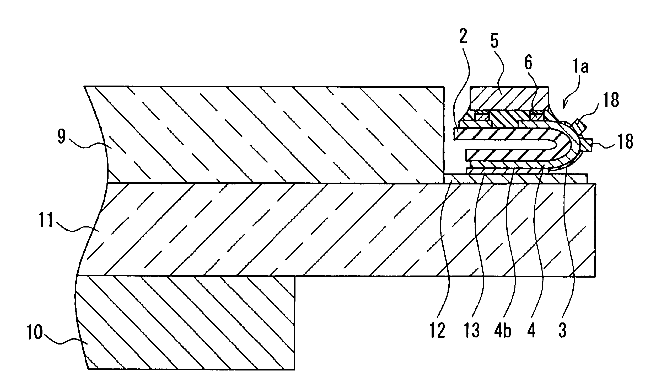
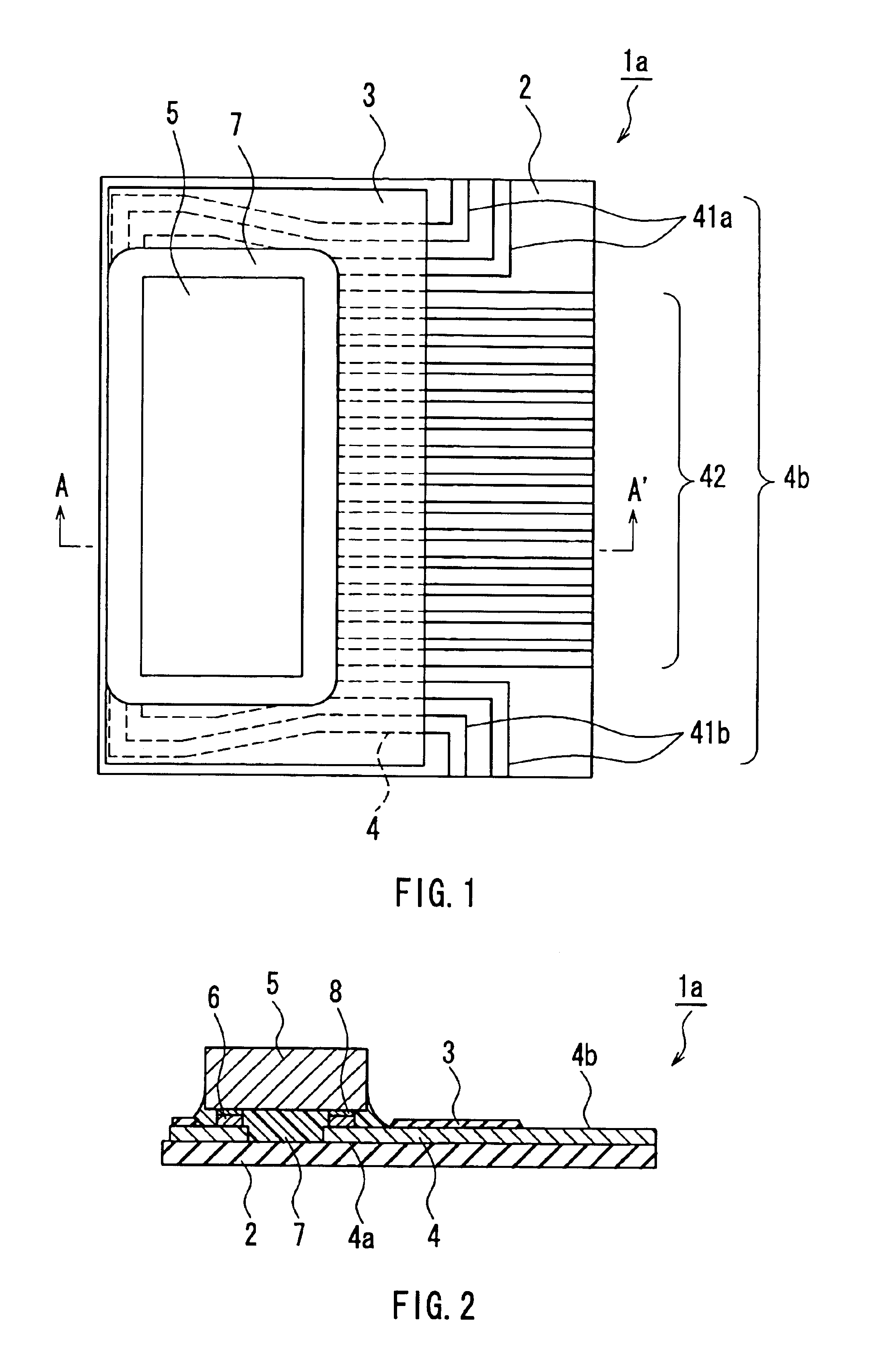
[0063]FIG. 1 is a plan view of a semiconductor device according to Embodiment 1 of the present invention, and FIG. 2 is a cross-sectional view taken along in the arrow direction of line A-A′ in FIG. 1. In a semiconductor device 1a, a semiconductor chip 5 is mounted on an insulating flexible film substrate 2 formed of a polyimide or the like, on which conductive leads 4 as wiring electrodes have been formed using a metal foil such as a copper foil. Metal electrodes 8 of the semiconductor chip 5 are connected to the conductive leads 4 via bumps 6 as protruding electrodes. The bumps 6 may have various heights. Also, it is possible to produce the semiconductor device without using the bumps 6. The conductive leads 4 typically are plated.

[0064]The space between the semiconductor chip 5 and the film su...

embodiment 2

(Embodiment 2)

[0091]A semiconductor device and a display device according to Embodiment 2 of the present invention will be described with reference to the accompanying drawings. FIG. 11 is a plan view of a semiconductor device according to Embodiment 2 of the present invention. A semiconductor device 1c according to Embodiment 2 has the same configuration as that of the semiconductor device 1a according to Embodiment 1 except that electronic-component-mounting regions 2a are provided on both ends of the region where the outer leads 4b are formed.

[0092]As shown in FIG. 11, the electronic-component-mounting regions 2a are portions where a solder resist 3 is formed so as to cover conductive leads 4. On the electronic-component-mounting regions 2a, electronic components 18, e.g., a capacitor and a resistor, are mounted. The electronic components 18 penetrate through the solder resist 3 to be joined to the conductive leads 4 with solder or the like.

[0093]In the following, the mounting of...

embodiment 3

(Embodiment 3)

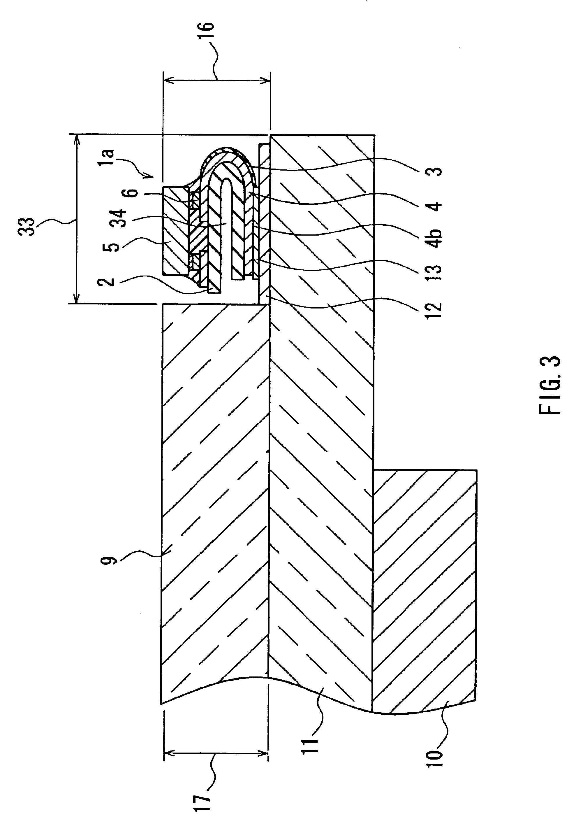
[0096]A semiconductor device and a display device according to Embodiment 3 of the present invention will be described with reference to the accompanying drawings. FIG. 14 is a cross-sectional view of a display device according to Embodiment 3 of the present invention. In the display device according to Embodiment 3, the semiconductor device 1a is mounted in the same manner as shown in FIG. 3 in Embodiment 1 except that a housing 25 provided in the display device is in intimate contact with the rear surface of the semiconductor chip 5. In the display device, illustration of the back light has been omitted. As the housing 25, a suitable member already provided in the display device may be used. Furthermore, as the housing 25, a material having a high thermal conductivity, such as aluminum, is preferable. In the display device having the above-described configuration, heat generated during the operation of the semiconductor chip 5 is transmitted to the housing 25 and dis...


PUM

PropertyMeasurementUnit
thicknessaaaaaaaaaa
thicknessaaaaaaaaaa
thicknessaaaaaaaaaa

Abstract

A semiconductor device to be mounted on an external electronic device includes a film substrate on which wiring electrodes are formed, the wiring electrodes being partially covered with a covering member; and a semiconductor chip mounted on the film substrate. In this semiconductor device, the film substrate is folded so that at least one edge of the film substrate is on a side opposite to a side on which the semiconductor chip is mounted, and portions of the wiring electrodes exposed from the covering member on a surface of the film substrate on which the semiconductor chip is mounted are to be connected to electrodes of an external electronic device.

Description

BACKGROUND OF THE INVENTION[0001]1. Field of the Invention[0002]The present invention relates to a semiconductor device of the tape carrier type and a display device including the same.[0003]2. Description of the Related Art[0004]Thin display devices typified by liquid crystal displays employ a semiconductor device for driving that inputs display signals. Such a semiconductor device is required to be thin and produce multiple output signals. Examples of the method of mounting such a semiconductor device include using a chip-on-glass (hereinafter, referred to as “COG”) structure or a tape-carrier-package (hereinafter, referred to as “TCP”) structure.[0005]First, a semiconductor device mounted on a display device so as to have a COG structure will be described. FIG. 24 is a cross-sectional view of a semiconductor device mounted on a display device so as to have a COG structure. A display glass 109 as a transparent substrate is adhered onto a glass substrate 111 as a display substrate ...

Claims


Application Information

Patent Timeline
Patent Type & Authority Patents(United States)
IPC IPC(8): G02F1/13H01L23/48H01L23/498G02F1/1345H01L21/60
CPCG02F1/13452H01L23/4985H01L2224/16H01L2924/01078H01L2224/16225H01L2224/32225H01L2224/73204H01L2924/00H01L24/05H01L2224/05568H01L2224/05573H01L2224/056H01L2924/00014
Inventor UENO, JUNICHITORII, MICHIHARUTANAKA, TAKAYUKI
Owner TESSERA ADVANCED TECH
Why Eureka
Try Eureka