Method of improving the stability of active matrix OLED displays driven by amorphous silicon thin-film transistors

a technology of amorphous silicon thin-film transistors and active matrix displays, which is applied in the direction of instruments, light sources, computing, etc., can solve the problems of inability to achieve long term stability of a-si tft driving devices on transistors, inability to achieve long term and inability to achieve the effect of long-term stability of a-si tft driving devices on transistors /

Inactive Publication Date: 2006-10-03
WINTEX
View PDF5 Cites 200 Cited by
  • Summary
  • Abstract
  • Description
  • Claims
  • Application Information

AI Technical Summary

Benefits of technology

[0013]Therefore this invention proposes an innovated way to improve the stability of a driving device for organic electric-excited light emitting transistor driven by amorphous silicon thin film transistor, the main purpose is to eliminate the non-uniformity of the threshold voltage Vth on thin film transistor, and extend life of the active matrix display panels.
[0014]Another purpose is to achieve the same result as in U.S. Pat. No. 6,677,713 without additional transistors or scan lines. That is, this invention involves a simpler system, which implies a lower cost for the manufacturers employing it.

Problems solved by technology

As a result of the continuous improvements in light emitting efficiency on OLED materials, using amorphous silicon thin-film transistor (a-Si TFT) as the driving platform for OLED devices is no longer infeasible.
Although a-Si TFT has absolute advantage of lower cost, there are still technical issues needed to improve if a-Si TFT is to be used to drive OLED.
Therefore long term stability of a-Si TFT driving devices on transistor 12 can not be achieved if conventional a-Si TFT driving circuitry is employed.
Therefore, the positive shift as a result of instability in threshold voltage, Vth, brings about two problems: The first is that the original brightness of OLED can not be maintained as a result of the decrease in output current on transistor 12, with time.
The second problem is that the degree of degradation on transistor 12 in the sub-pixel varies with time.
In other words, a set of scan driver need to be added to the system which will increase the complexity in manufacturing and, with the additional driving circuitry, substantially increase its cost.

Method used


Image

  • Method of improving the stability of active matrix OLED displays driven by amorphous silicon thin-film transistors
  • Method of improving the stability of active matrix OLED displays driven by amorphous silicon thin-film transistors
  • Method of improving the stability of active matrix OLED displays driven by amorphous silicon thin-film transistors

Examples


Embodiment Construction

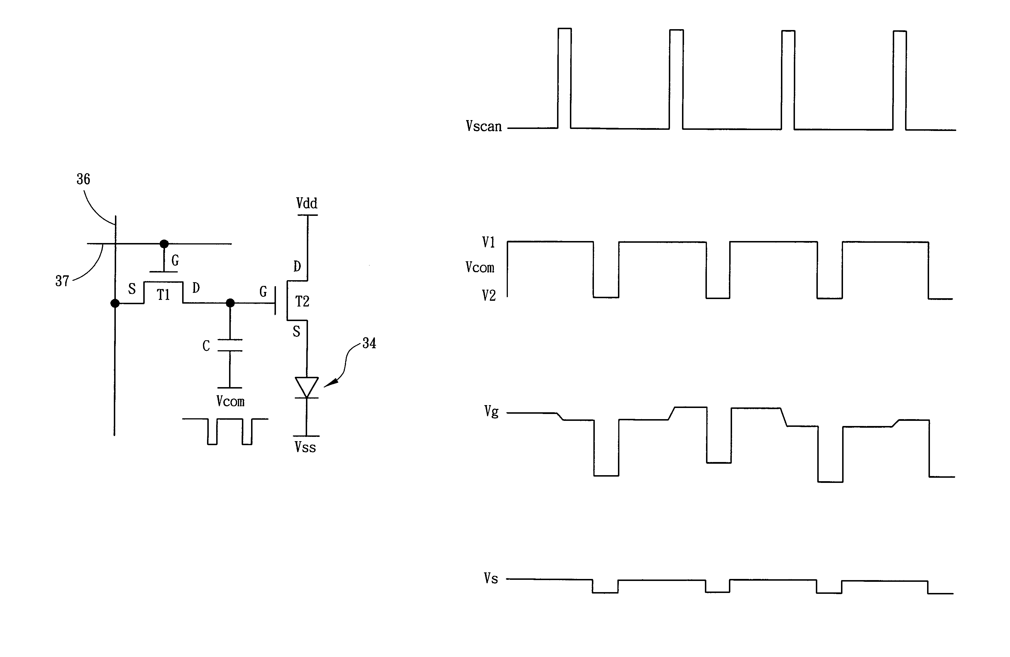
[0030]The driving circuitry for each sub-pixel in this invention and the schematic diagram of the connection as well as control of each sub-pixel on display panel are shown in FIGS. 6 and 7. As shown in the figures, each data line 36 and each scan line 37 on the display device form a matrix of m×n sub-pixels on the display panel. The driving circuitry for each sub-pixel includes two TFT and a capacitance. The organic light emitting diode (OLED) 34 is driven by a driving transistor T2, the drain (D) of which is connected to the power source Vdd, and the source (S) to the anode of the organic light emitting diode 34. The cathode of the organic light emitting diode 34 is connected to a comparatively fixed low potential Vss (for example to the ground as zero potential). Besides, the gate (G) of a scanning transistor is connected to scan line 37, the source (S) is connected to data line 36, and the drain (D) to the gate (G) of driving transistor T2 and one end of storage capacitance. In ...


PUM


Abstract

A method of improving the stability of organic light emitting diode (OLED) display devices driven by amorphous silicon thin-film transistors, in which the driving circuitry within each sub-pixel includes a driving transistor for driving organic light emitting diode (OLED), a scanning transistor and a storage capacitance. An end of the capacitance is connected to the signal resetting line, which a resetting time pulse of high potential and low potential are supplied. Since the resetting signals within the sub-pixels are synchronized, a single voltage of the resetting signal can control the positive and negative stresses for each transistor in the sub-pixels on the panel.

Description

FILED OF THE INVENTION[0001]The present invention is about driving an amorphous silicon thin-film transistor, more particularly driving an organic light emitting diode (OLED) display, to enhance the stability of the threshold voltage (Vth) as a function of time on the amorphous silicon thin-film transistors.BACKGROUND OF THE INVENTION[0002]There are two ways to drive an organic light emitting display (OLED): one is passive matrix driving and the other is active matrix driving. In an active matrix device, a good service life and high resolution can be achieved without being driven to an extremely high brightness. Therefore, OLED combined with thin-film transistor (TFT) to realize the active matrix technology conforms to the present market requirements for fluidity of images as well as higher and higher resolution in display panels that fully demonstrate the superior properties of OLED. As a result of the continuous improvements in light emitting efficiency on OLED materials, using am...

Claims


Application Information

Patent Timeline
Patent Type & Authority Patents(United States)
IPC IPC(8): G09G3/10
CPCG09G3/3233G09G2300/0842G09G2300/0876G09G2310/0254G09G2320/0233G09G2320/043
Inventor LO, SHIN-TAIHSU, CHING-FU
Owner WINTEX
Why Eureka
Try Eureka