Pixel circuit for active matrix OLED and driving method

a technology of active matrix and oled, which is applied in the direction of identification means, instruments, static indicating devices, etc., can solve the problems of large variation in the threshold voltage of tft, shorten the life-time of oled, and poor uniformity of illumination, so as to avoid large current generation and ir-drop

Active Publication Date: 2006-04-04
IND TECH RES INST
View PDF6 Cites 199 Cited by
  • Summary
  • Abstract
  • Description
  • Claims
  • Application Information

AI Technical Summary

Benefits of technology

[0017]A pixel circuit for active matrix OLED and driving method is proposed in this invention, it use a first-transistor connect to a control line to let a second transistor which connect to the former scan line cut-off when writing a low voltage in, so to avoid large current generation and IR-drop.

Problems solved by technology

The problem which pixel circuit of prior art is the threshold voltage of TFT has big variation.
Finally, the uniformity of illumination isn't well.
It causes shorten the life-time of OLED and worse image quality, and operation complex because it need to provide a low voltage before writing correct data in data driving circuit.

Method used


Image

  • Pixel circuit for active matrix OLED and driving method
  • Pixel circuit for active matrix OLED and driving method
  • Pixel circuit for active matrix OLED and driving method

Examples


Embodiment Construction

[0029]Reference will now be made in detail to the preferred embodiments of the present invention, examples of which are illustrated in the accompanying drawings. Wherever possible, the same reference numbers are used in the drawings and the description to refer to the same or like parts.

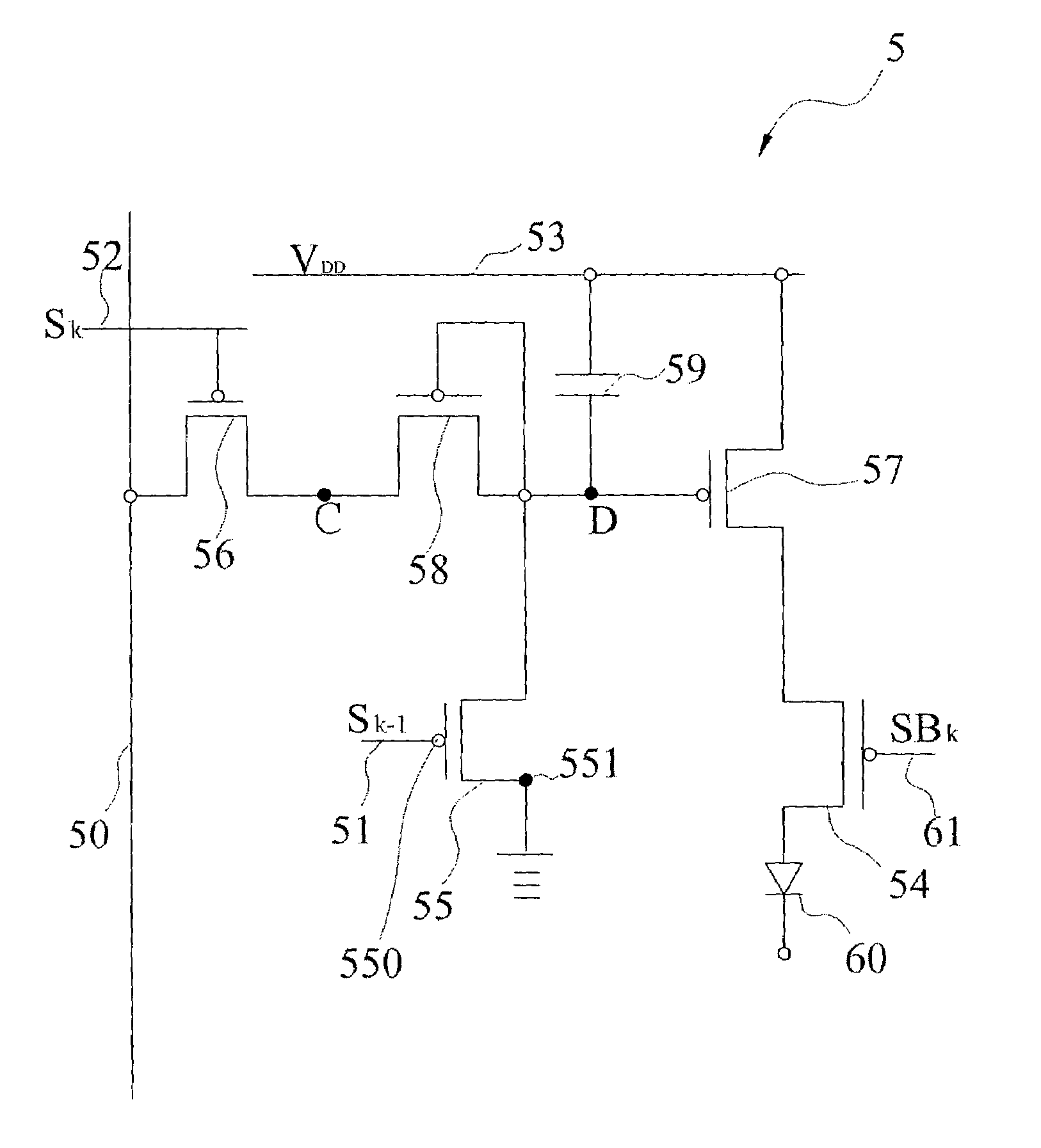
[0030]Refer to FIG. 5 is an illustrated view showing a pixel circuit 5 in accordance to an embodiment of the present invention, wherein includes a data line 50, a former scan line 51, a scan line 52, a signal line 53, the first transistor 54, the second transistor 55, the third transistor 56, the fourth transistor 57, the fifth transistor 58 and a storage capacitance 59.

[0031]The function of the first transistor is a switch which received control signal SBK output by control line 61 to cut-off the first transistor 54; the second transistor 55 which received scan signal SK−1 output by former scan line 51 and provide a low voltage to saturate the fifth transistor 58. The gate 550 of the second transist...


PUM


Abstract

A pixel circuit for active matrix OLED and driving method is proposed in this invention, which includes five transistors and one capacitance, it's mainly use a first-transistor connected to a control line to let a second transistor connected to the former scan line off when writing a low voltage in, so to avoid large current generation and IR-drop, finally the illumination will be more uniform than prior art.

Description

BACKGROUND OF THE INVENTION[0001]1. Field of the Invention[0002]The present invention relates to a pixel circuit for active matrix OLED and driving method which provide the illumination uniformity.[0003]2. Description of the Related Art[0004]Organic light emitting devices is a new light emitting technology, its principle is a sandwich structure that organic film to place in between two electrode layers. The light need transparent to device, so one of electrodes needs to use ITO electrode. When drive a forward bias to device between anode and cathode, the electron and hole that generated by anode and cathode will empty into light emitting material and then emit light by radiation and re-combine method.[0005]The major application of Organic Light Emitting Devices is display, the pixel circuit is similar with the circuit of TFT LCD, they are all matrix arrays. An illustrated view showing a pixel circuit of Organic Light Emitting Devices of the prior art is shown as FIG. 1. After scan l...

Claims


Application Information

Patent Timeline
Patent Type & Authority Patents(United States)
IPC IPC(8): G09G3/32G09F9/30G09G3/20H01L51/50G09G3/30H01L27/32H05B33/14
CPCG09G3/3233G09G2300/0809G09G2300/0819G09G2320/043G09G2300/0861G09G2310/0251G09G2300/0842
Inventor CHEN, CHIEN-RUCHEN, SHANG-LISHIH, JUN-REN
Owner IND TECH RES INST
Why Eureka
Try Eureka