Method of manufacturing charge storage device

a charge storage and manufacturing method technology, applied in semiconductor devices, capacitors, electrical devices, etc., can solve the problems of increasing the surface area of metal electrodes that are not so easy, and achieve the effects of reducing production costs, simplifying manufacturing processes, and increasing charge storage capacity

Inactive Publication Date: 2008-07-29
IND TECH RES INST
View PDF4 Cites 413 Cited by
  • Summary
  • Abstract
  • Description
  • Claims
  • Application Information

AI Technical Summary

Benefits of technology

[0007]Accordingly, at least one objective of the present invention is to provide a method of manufacturing a charge storage device capable of increasing the lower electrode area of the charge storage device.
[0008]At least another objective of the present invention is to provide a method of manufacturing a charge storage device capable of simplifying the production process and miniaturize the device.
[0025]In the method of manufacturing a charge storage device according to the present invention, the capacity of an atomic layer deposition process for a precise control of the thickness and material composition of a deposited film is utilized to form a gradually-changed stacked insulation layer. Then, using the difference in etching rates as a result of the gradual change in the material composition, the etched sidewalls of the stacked insulation layer can have an uneven profile. Ultimately, the charge storage device formed on the gradual stacked insulation layer can have a larger charge storage capacity.
[0026]Furthermore, all the steps for manufacturing the charge storage device according to the present invention are performed inside a single reaction chamber. By adjusting the composition of the precursor material (the reactive gases) or the reaction time, the required stacked insulation layer (the gradual material layer) is formed. Therefore, the manufacturing process is simplified and the production cost is reduced.

Problems solved by technology

Although using a metal electrode has the advantage of a lower dielectric response, but increasing the surface area of the metal electrode is not so easy.

Method used


Image

  • Method of manufacturing charge storage device
  • Method of manufacturing charge storage device
  • Method of manufacturing charge storage device

Examples


Embodiment Construction

[0031]Reference will now be made in detail to the present preferred embodiments of the invention, examples of which are illustrated in the accompanying drawings. Wherever possible, the same reference numbers are used in the drawings and the description to refer to the same or like parts.

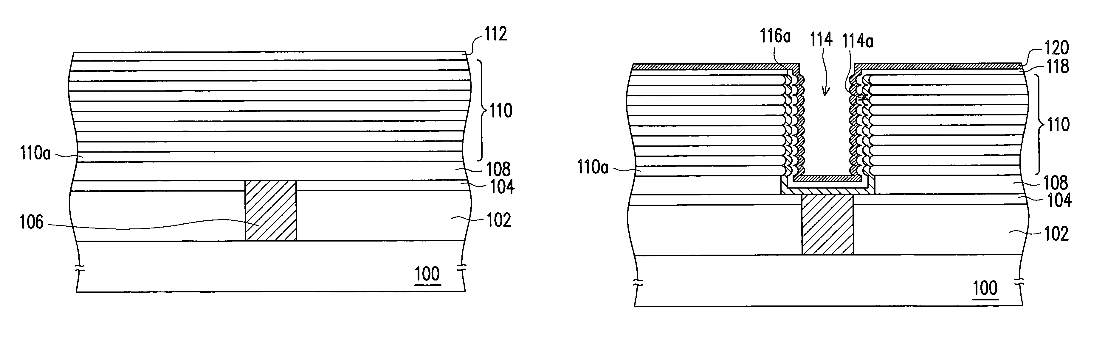
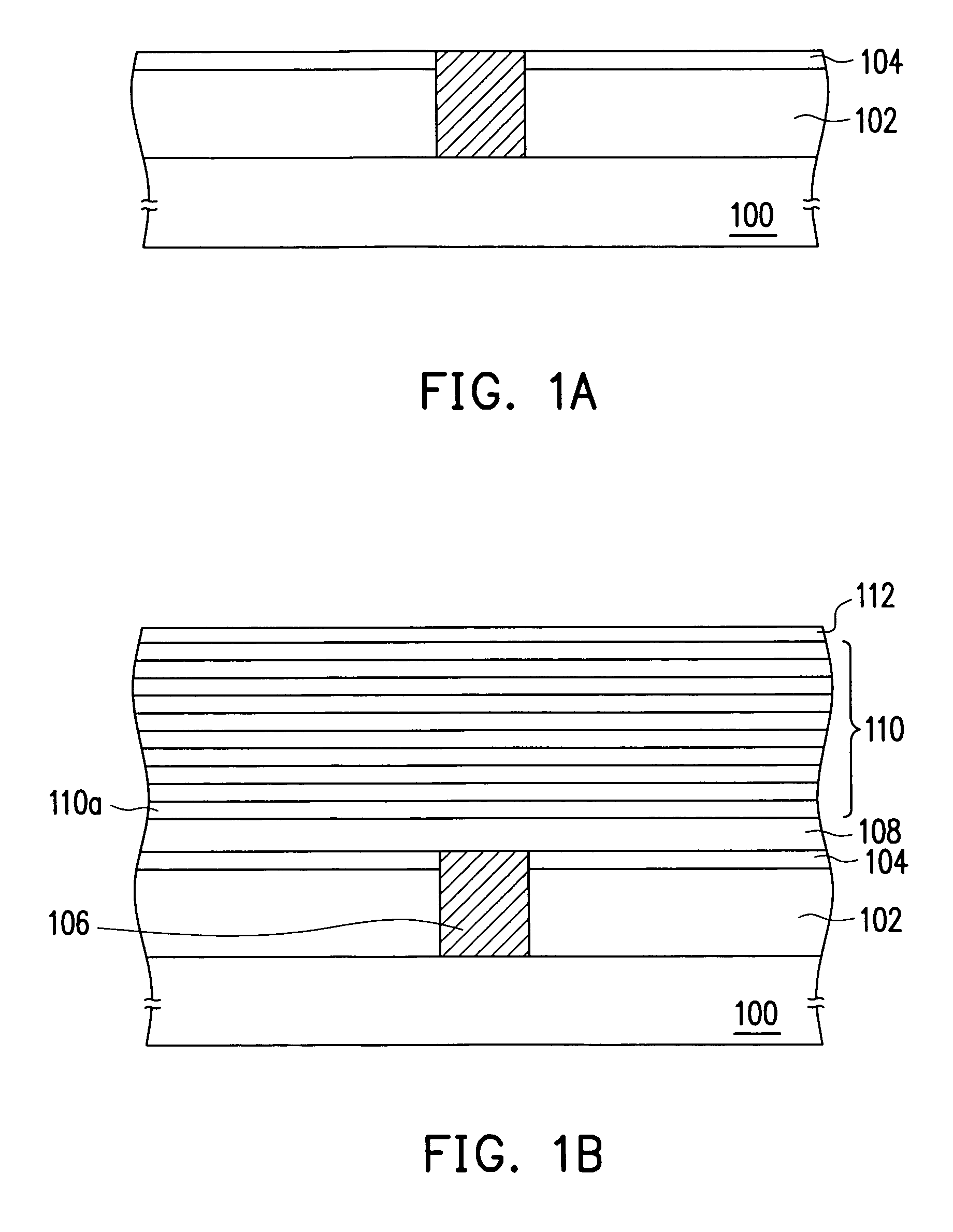
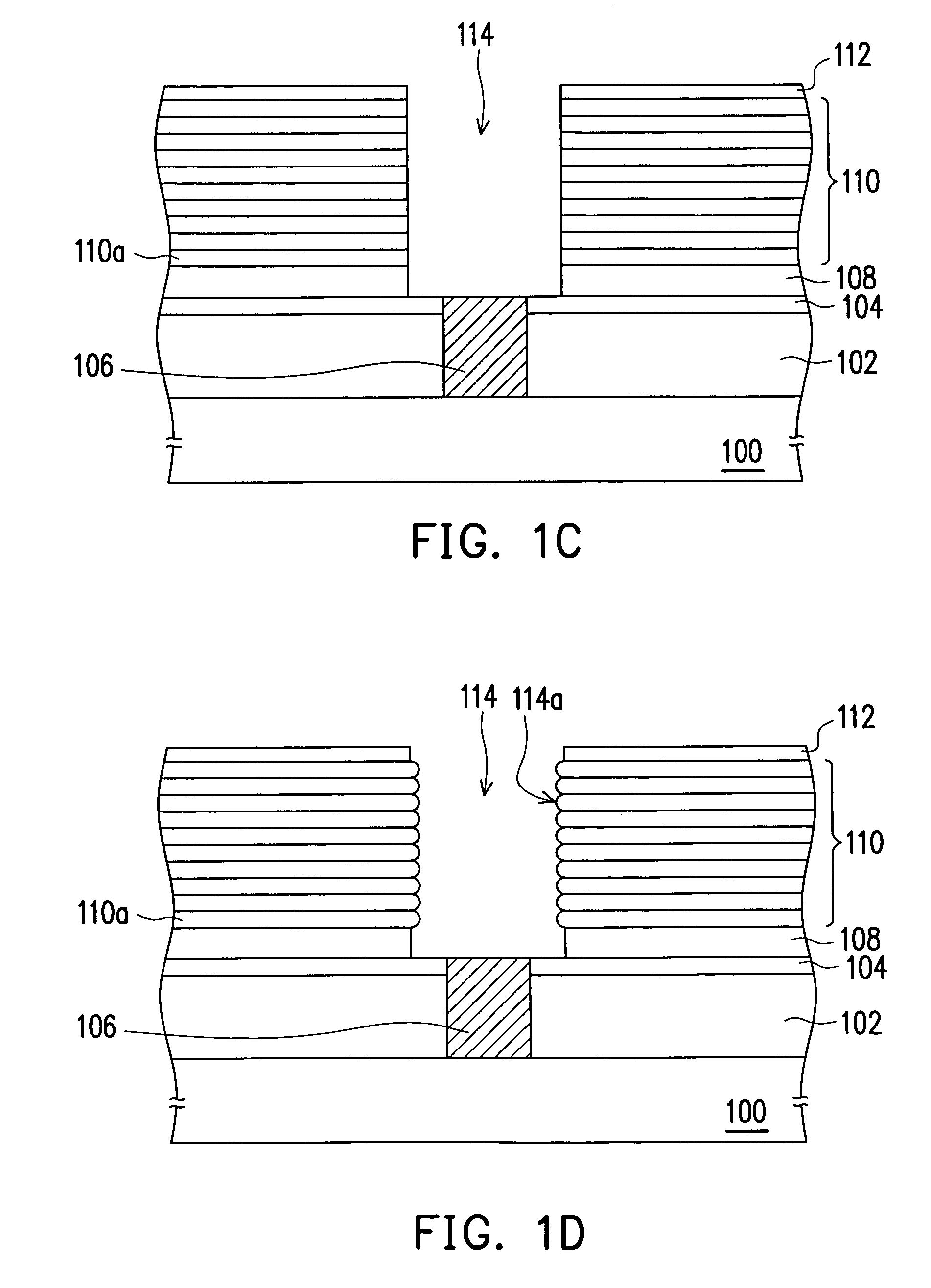
[0032]FIGS. 1A to 1F are schematic cross-sectional views showing the steps for forming a charge storage device according to the present invention. FIG. 2 is a graph showing the relation between the ratio of silicon in the HfxSiyOz and the thickness of the gradual material layer and the relation between the etching rate and the thickness of the gradual material layer.

[0033]First, as shown in FIG. 1A, a substrate 100 is provided. The substrate 100 is a silicon substrate (for a simpler view, the device within the substrate 100 are not shown), for example. Then, an insulation layer 102 and a cap layer 104 are formed on the substrate 100. The insulation layer 102 is fabricated using silicon oxide, for exa...


PUM

PropertyMeasurementUnit
dielectric constantaaaaaaaaaa
thicknessaaaaaaaaaa
thicknessaaaaaaaaaa

Abstract

A method of manufacturing a charge storage device is provided. Utilizing the capacity for a precise control of the thickness and the silicon content of a deposited film in an atomic layer deposition process, a stacked gradual material layer such as a hafnium silicon oxide (HfxSiyOz) layer is formed. The silicon content is gradually changed throughout the duration of the HfxSiyOz deposition process. The etching rate for the HfxSiyOz layer in dilute hydrogen fluoride solution is dependent on the silicon content y in the HfxSiyOz layer. The sidewalls of the stacked gradual material layer are etched to form an uneven profile. The lower electrode, the capacitor dielectric layer and the upper electrode are formed on the uneven sidewalls of the stacked gradual material layers, the area between the lower electrode and the upper electrode is increased to improve the capacitance of the charge storage device.

Description

CROSS-REFERENCE TO RELATED APPLICATION[0001]This application claims the priority benefit of Taiwan application serial no. 95100872, filed on Jan. 10, 2006. All disclosure of the Taiwan application is incorporated herein by reference.BACKGROUND OF THE INVENTION[0002]1. Field of the Invention[0003]The present invention relates to a method of manufacturing a semiconductor device. More particularly, the present invention relates to a method of manufacturing a charge storage device.[0004]2. Description of the Related Art[0005]As the techniques for manufacturing deep sub-micron semiconductor devices start to mature, the size of each device is reduced correspondingly. Hence, for a dynamic random access memory, the area assigned to each memory cell for disposing the capacitor has become smaller and smaller. On the other hand, with the increasing demand for a larger storage space for computer application software, memory with an ever-increasing storage capacity is required. As the conflictin...

Claims


Application Information

Patent Timeline
Patent Type & Authority Patents(United States)
IPC IPC(8): H01L21/31H01L29/792
CPCH01L21/31111H01L21/3142H01L28/84H01L27/10852H01L21/31625H01L21/02274H01L21/02164H01L21/02148H01L21/022H01L21/0228H01L21/02159H01L21/0217H10B12/033
Inventor LIANG, CHIEH-SHUOTZENG, PEI-JERLEE, HENG-YUANLEE, LURNG-SHEHNG
Owner IND TECH RES INST
Why Eureka
Try Eureka