Field effect transistor having vertical channel structure

a field effect transistor and vertical channel technology, applied in transistors, electrical devices, semiconductor devices, etc., can solve the problems of limited on resistance reduction, difficult to produce them at low cost, and increased chip area, so as to achieve high breakdown voltage, high breakdown electric field strength, and wide band gap

Inactive Publication Date: 2008-10-21
PANASONIC CORP
View PDF4 Cites 11 Cited by
  • Summary
  • Abstract
  • Description
  • Claims
  • Application Information

AI Technical Summary

Benefits of technology

[0015]An object of the present invention is to provide a field effect transistor with a lower on resistance and a vertical channel structure and to provide a method for manufacturing the field effect transistor.
[0016]Specifically, the invention is directed to a vertical channel field effect transistor, which is composed of, for example, a group III nitride semiconductor and which has a lower on resistance resulting from the reduction of a contact resistance at a source or drain electrode reduced by increasing the area of the electrode when compared with the cross-sectional area of the vertical channel, and to provide a method for manufacturing the field effect transistor including a epitaxial regrowth process.

Problems solved by technology

Because of this, when the horizontal channel transistor structure is applied to large-current transistor, problems arise in that their chip area is increased and it is difficult to produce them at low cost.
As a result, reduction of the on resistance is limited by the large electrode contact resistance.

Method used


Image

  • Field effect transistor having vertical channel structure
  • Field effect transistor having vertical channel structure
  • Field effect transistor having vertical channel structure

Examples


first embodiment

[0073]A first embodiment according to the present invention will be described below with reference to the drawings.

[0074]A field effect transistor having a vertical channel and a method for manufacturing the same according to the first embodiment have the following feature: a first insulating film, a gate electrode, and a second insulating film are selectively formed on a first n-type contact semiconductor layer in that order, and then an stripe-shaped opening is formed in the multilayer film structure comprised of the three layers; an undoped channel semiconductor layer and a second n-type contact semiconductor layer are formed via the opening so that both the layers are regrown by, for example, metal organic chemical vapor deposition; a drain electrode is formed so that the drain electrode contacts the first n-type contact semiconductor layer; a source electrode is formed so that the source electrode contacts the second n-type contact semiconductor layer; and the regrowth undoped ...

second embodiment

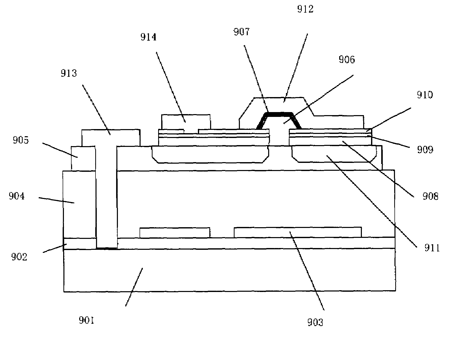
[0139]A second embodiment according to the invention will be described with reference to FIG. 9.

[0140]FIG. 9 is a cross-sectional view of a field effect transistor with a vertical channel according to the second embodiment of the invention. In FIG. 9, reference numeral 901 denotes a conductive Si substrate, reference numeral 902 an AlN buffer layer, reference numeral 903 a SiO2 mask layer, reference numeral 904 a first undoped GaN layer, reference numeral 905 a n+-type GaN layer (first contact semiconductor layer), reference numeral 906 a second undoped GaN layer (channel semiconductor layer), reference numeral 907 a n+-type InAlGaN layer (second contact semiconductor layer), reference numeral 908 a first SiO2 thin film, reference numeral 909 a tungsten gate electrode, reference numeral 910 a second SiO2 thin film, reference numeral 911 a high-resistance region, reference numeral 912 a Ti / Al / Ni / Au source electrode, reference numeral 913 a Ti / Al / Ni / Au drain electrode, and reference n...

third embodiment

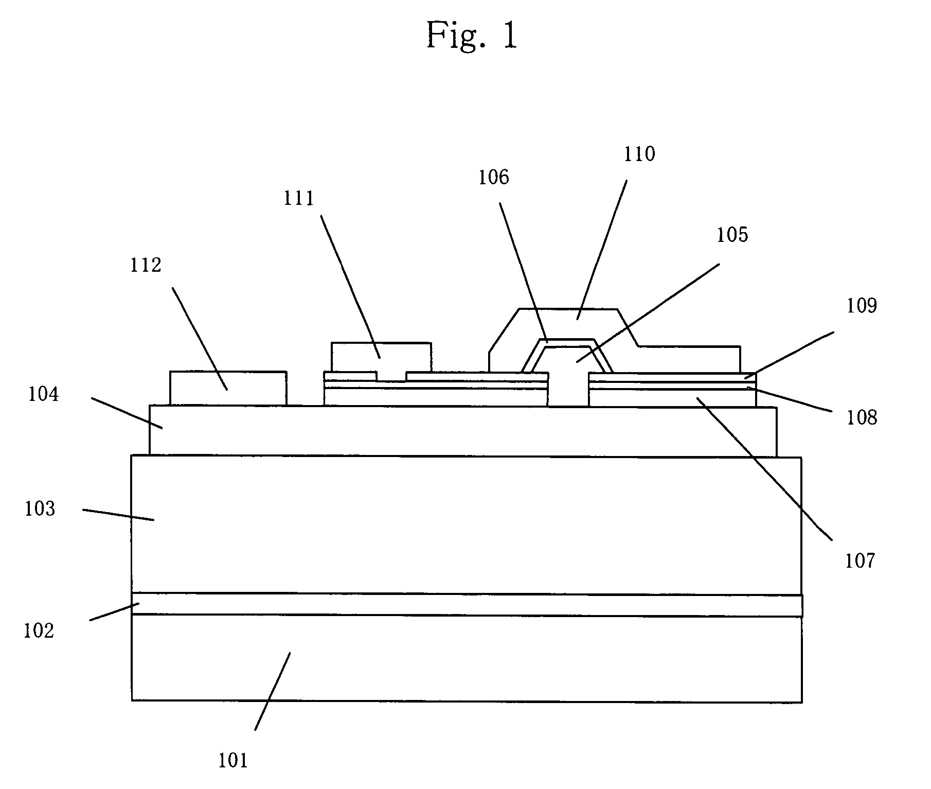
[0156]A third embodiment according to the invention will be described with reference to FIGS. 10 to 12.

[0157]FIG. 10 is a cross-sectional view of a field effect transistor having a vertical channel according to the third embodiment of the invention. In FIG. 10, reference numeral 1001 denotes a sapphire substrate, reference numeral 1002 an AlN buffer layer, reference numeral 1003 a first undoped GaN layer, reference numeral 1004 a first n+-type GaN layer (first contact semiconductor layer), reference numeral 1005 a second undoped GaN layer (channel semiconductor layer), reference numeral 1006 a second n+-type GaN layer (second contact semiconductor layer), reference numeral 1007 a first SiO2 thin film, reference numeral 1008 an ITO gate electrode, reference numeral 1009 a second SiO2 thin film, reference numeral 1010 a Ti / Al / Ni / Au source electrode having Au / plate wiring on its top surface, reference numeral 1011 a Ti / Au gate pad electrode, reference numeral 1012 a Ti / Al / Ni / Au drain e...


PUM


Abstract

A first SiO2 thin film, a tungsten gate electrode, and a second SiO2 thin film are selectively formed on a first n+-type GaN contact semiconductor layer in that order and in a multilayer film structure having the three layers, a stripe-shaped opening is formed. Via the opening, an undoped GaN channel semiconductor layer and the second n+-type GaN contact semiconductor layer are formed so that both the layers are regrown by, for example, metal organic chemical vapor deposition. A source electrode and a drain electrode are formed so as to contact the corresponding second and first n+-type GaN contact semiconductor layers. The regrown undoped GaN channel semiconductor layer and the regrown second n+-type GaN contact semiconductor layer are horizontally grown portions and hence, the contact area of the electrode can be made larger than the area of the opening.

Description

BACKGROUND OF THE INVENTION[0001]1. Field of the Invention[0002]The present invention relates to a field effect transistor having a vertical channel which uses, for example, a nitride semiconductor and to a manufacturing method for the field effect transistor. This field effect transistor can be applied to, for example, high-power transistors used in power supply circuits of consumer electronics and to high-frequency transistors used in transmitting and receiving circuits of cellular telephones, extremely high-frequency radars, and the like.[0003]2. Background Art[0004]Group III nitride compound semiconductors represented by GaN have characteristics in that since the band gaps of GaN and AlN are as high as 3.4 eV and 6.2 eV at room temperature respectively, they have high breakdown electric field strength and that the saturated drift velocity of their electrons is high when compared with that of compound semiconductors such as GaAs or Si semiconductors. Because of this, the group II...

Claims


Application Information

Patent Timeline
Patent Type & Authority Patents(United States)
IPC IPC(8): H01L29/76
CPCH01L29/66856H01L29/8122H01L29/2003
Inventor UEDA, TETSUZO
Owner PANASONIC CORP
Why Eureka
Try Eureka