Nitride semiconductor laser device

Active Publication Date: 2009-06-04
ROHM CO LTD
View PDF3 Cites 230 Cited by
  • Summary
  • Abstract
  • Description
  • Claims
  • Application Information

AI Technical Summary

Benefits of technology

[0012]An object of the present invention is to provide a nitride semiconductor laser device capable of improving life characteristics by relaxing stress resulting from an elec

Problems solved by technology

If a large quantity of dopant is present near the light emitting layer, however, emission loss is disadvantageously increased.
This

Method used


Image

  • Nitride semiconductor laser device
  • Nitride semiconductor laser device
  • Nitride semiconductor laser device

Examples


Embodiment Construction

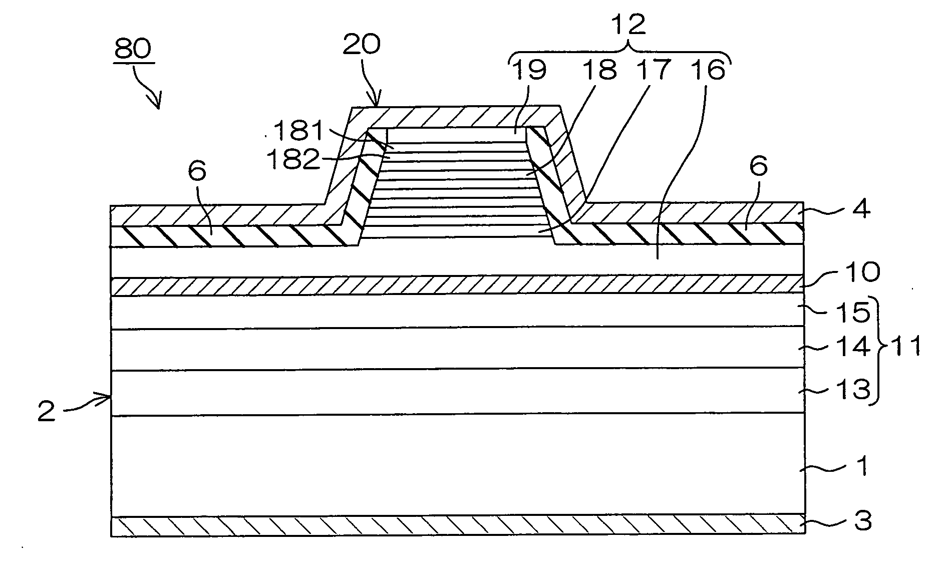
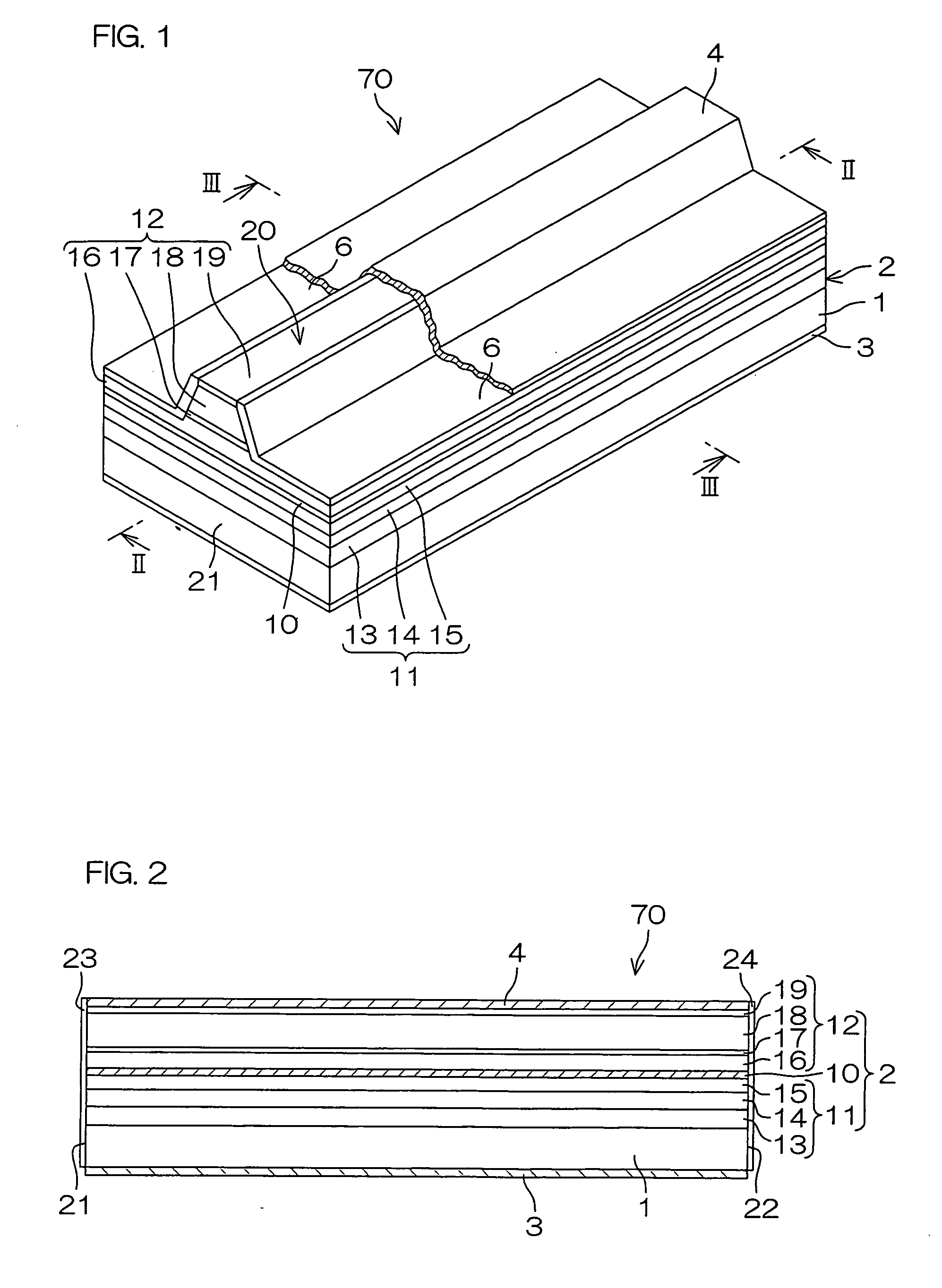
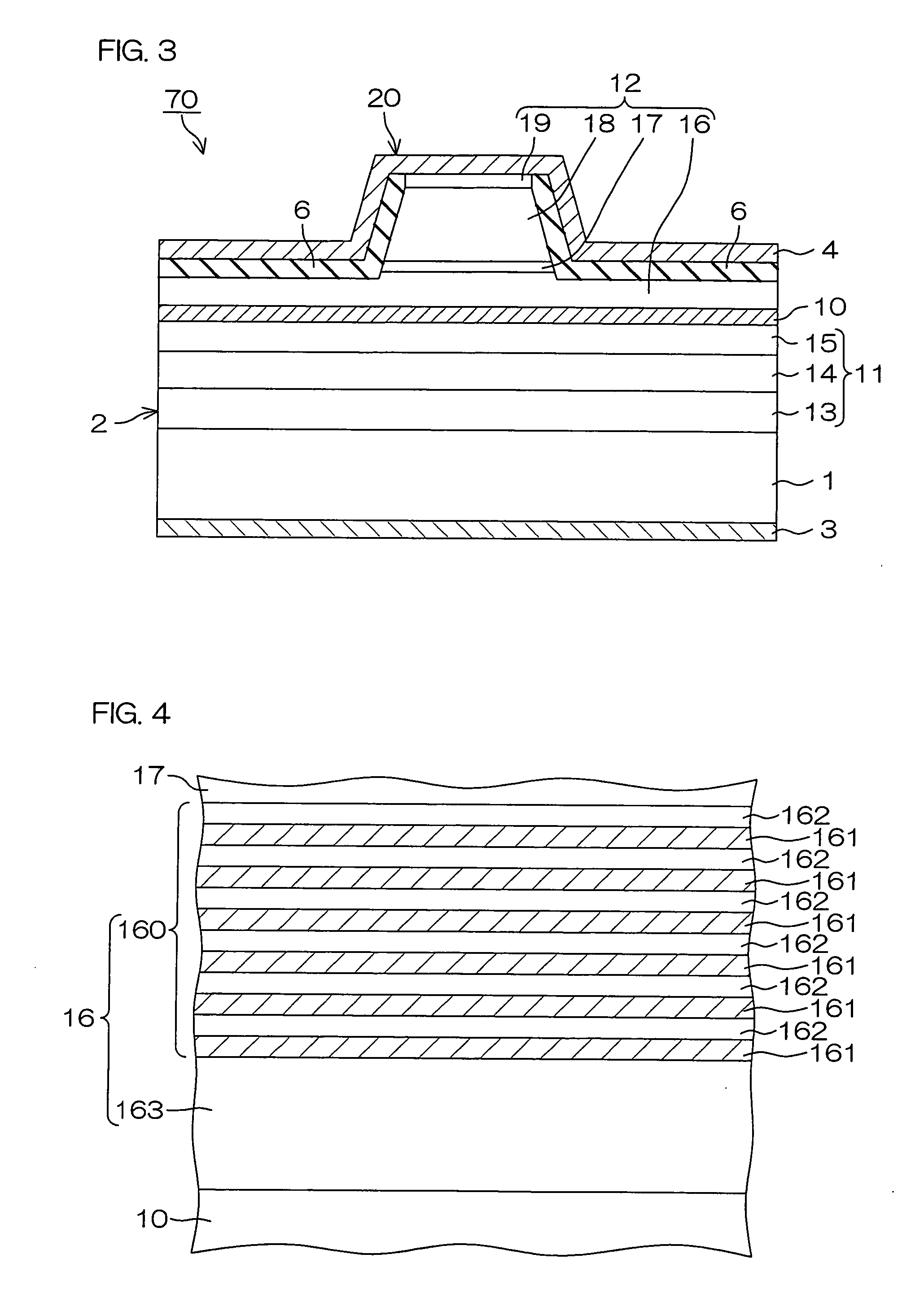
[0022]A nitride semiconductor laser device according to an embodiment of the present invention has a group III nitride semiconductor multilayer structure. This group III nitride semiconductor multilayer structure includes an n-type semiconductor layer, a p-type semiconductor layer and a light emitting layer held between the n-type semiconductor layer and the p-type semiconductor layer, and the p-type semiconductor layer is formed by successively stacking a p-side guide layer, a p-type electron blocking layer in contact with the p-side guide layer and a p-type cladding layer in contact with the p-type electron blocking layer from the side closer to the light emitting layer. The p-side guide layer is formed by stacking a layer made of a group III nitride semiconductor containing Al and a layer made of a group III nitride semiconductor containing no Al. The p-type cladding layer is made of a group III nitride semiconductor containing Al, and the p-type electron blocking layer is made o...


PUM


Abstract

A nitride semiconductor laser device has a group III nitride semiconductor multilayer structure. The group III nitride semiconductor multilayer structure includes an n-type semiconductor layer, a p-type semiconductor layer and a light emitting layer held between the n-type semiconductor layer and the p-type semiconductor layer, and the p-type semiconductor layer is formed by successively stacking a p-side guide layer, a p-type electron blocking layer in contact with the p-side guide layer and a p-type cladding layer in contact with the p-type electron blocking layer from the side closer to the light emitting layer. The p-side guide layer is formed by stacking a layer made of a group III nitride semiconductor containing Al and a layer made of a group III nitride semiconductor containing no Al. The p-type cladding layer is made of a group III nitride semiconductor containing Al, and the p-type electron blocking layer is made of a group III nitride semiconductor having a larger Al composition than the p-type cladding layer.

Description

BACKGROUND OF THE INVENTION[0001]1. Field of the Invention[0002]The present invention relates to a nitride semiconductor laser device including a nitride semiconductor multilayer structure made of group III nitride semiconductors.[0003]2. Description of Related Art[0004]Group III-V semiconductors employing nitrogen as a group V element are referred to as “group III nitride semiconductors”, and typical examples thereof include aluminum nitride (AlN), gallium nitride (GaN) and indium nitride (InN), which can be generally expressed as AlxInyGa1-X-YN (0≦X≦1, 0≦Y≦1 and 0≦X+Y≦1).[0005]A short wavelength laser source emitting a blue or green laser beam is increasingly employed in the fields of high-density recording in an optical disk represented by a DVD, image processing, medical instruments, measuring instruments and the like. Such a short wavelength laser source is constituted of a laser diode employing GaN semiconductors, for example.[0006]A GaN semiconductor laser diode is manufactur...

Claims


Application Information

Patent Timeline
IPC IPC(8): H01S5/30
CPCB82Y20/00H01S5/028H01S5/0287H01S5/2009H01S2304/04H01S5/305H01S5/3063H01S5/3216H01S5/34333H01S5/22
Inventor KOHDA, SHINICHINAKAGAWA, DAISUKE
Owner ROHM CO LTD
Why Eureka
Try Eureka