Compound for organic optoelectronic device, organic light emitting diode including the same and display including the organic light emitting diode

a technology of optoelectronic devices, which is applied in the direction of luminescent compositions, organic chemistry, chemistry apparatus and processes, etc., can solve the problems of inefficient combination of holes and electrons, the development of organic material layer forming materials for organic light emitting diodes has so far not been satisfactory, etc., to improve life-span characteristics, high hole or electron transport properties, and thermal stability

Active Publication Date: 2015-06-11
SAMSUNG SDI CO LTD
View PDF9 Cites 24 Cited by
  • Summary
  • Abstract
  • Description
  • Claims
  • Application Information

AI Technical Summary

Benefits of technology

[0045]A compound having high hole or electron transport properties, film stability, thermal stability, and high triplet exciton energy may be provided.
[0046]Such a compound may be used as a hole injection / transport material, host material, or electron injection / transport material of an emission layer. An organic optoelectronic device using the same has improved life-span characteristics, and high luminous efficiency at a low driving voltage due to excellent electrochemical and thermal stability.

Problems solved by technology

However, development of an organic material layer forming material for an organic light emitting diode has thus far not been satisfactory and thus there is a need for a novel material.
However, since an organic material in general has slower electron mobility than hole mobility, it has a drawback of inefficient combination between holes and electrons.

Method used


Image

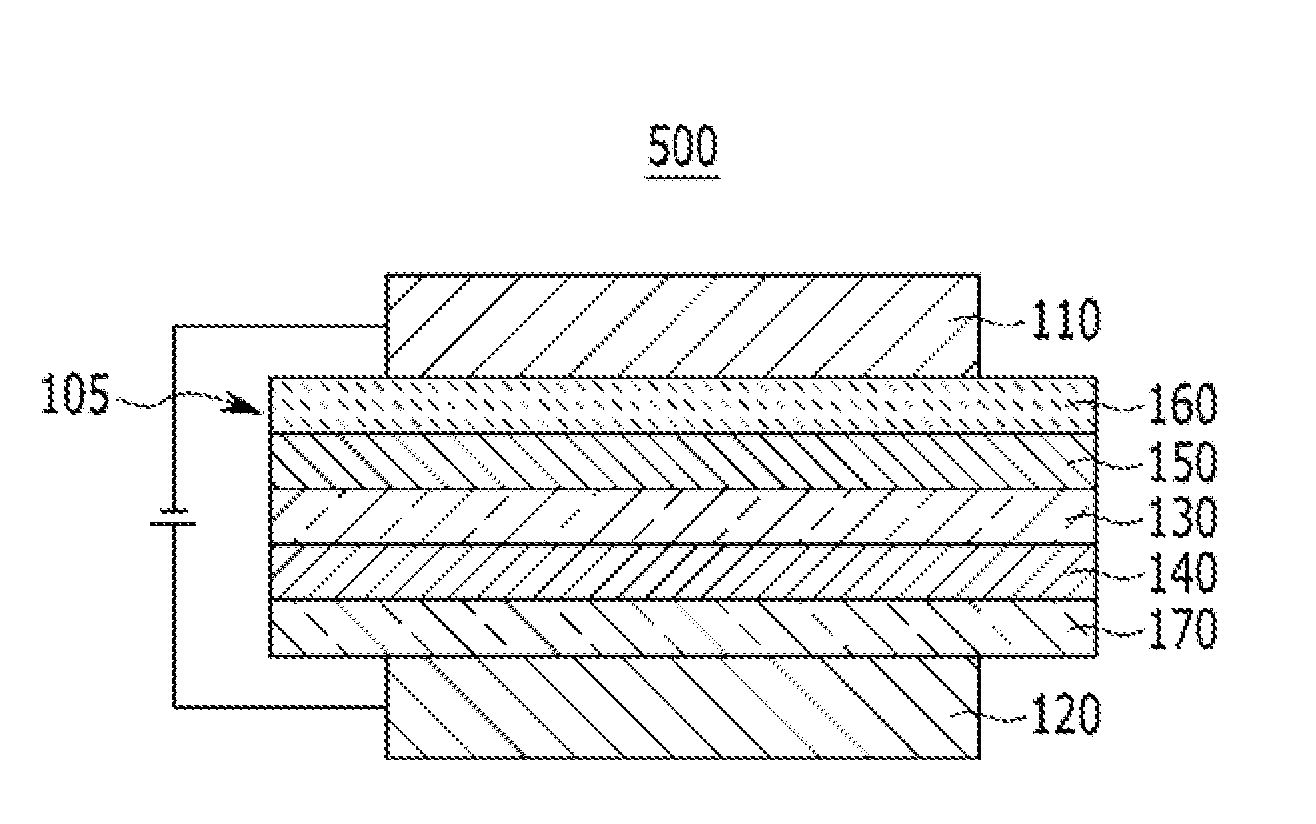
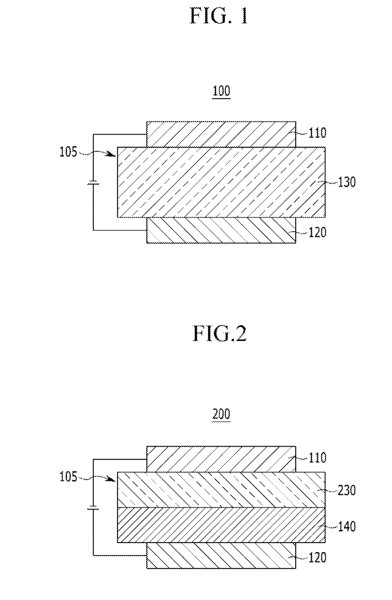
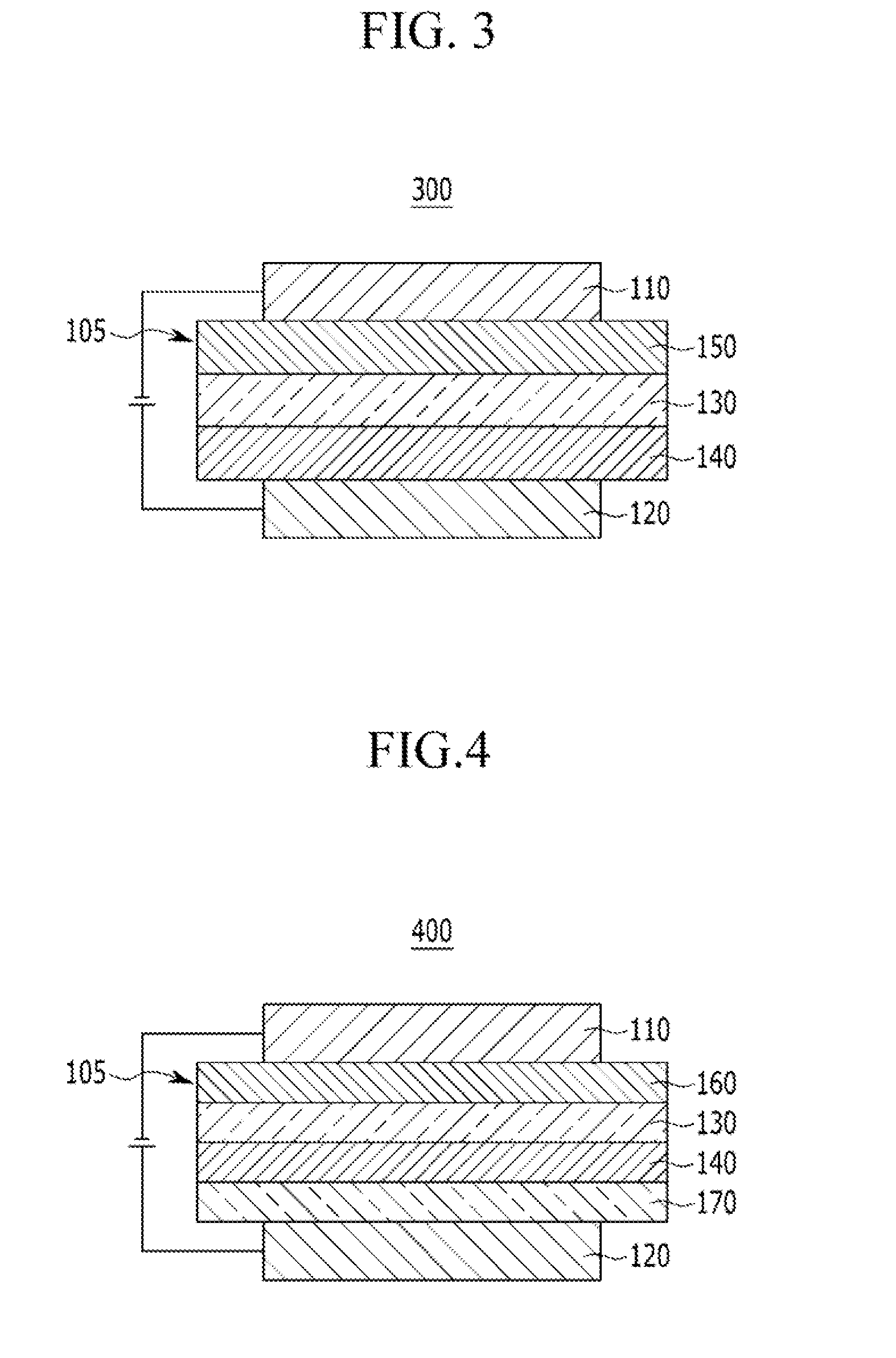
  • Compound for organic optoelectronic device, organic light emitting diode including the same and display including the organic light emitting diode
  • Compound for organic optoelectronic device, organic light emitting diode including the same and display including the organic light emitting diode
  • Compound for organic optoelectronic device, organic light emitting diode including the same and display including the organic light emitting diode

Examples


example 1

Preparation of Compound Represented by Chemical Formula C-143

[0209]

[0210]10 g (30.59 mmol) of the intermediate M-1, 9.8 g (30.59 mmol) of bis-biphenyl-4-yl-amine, and 3.8 g (39.8 mmol) of sodium t-butoxide were put in a round-bottomed flask, 200 mL of toluene was added, 0.19 g (0.92 mmol) of tri-tert-butylphosphine and 0.18 g (0.31 mmol) of Pd(dba)2 were added, and the resultant was agitated under a nitrogen atmosphere for 12 hours at 100° C. When the reaction was terminated, the resultant was extracted with toluene and distilled water, the organic layer was dried with magnesium sulfate, and filtered, and then the filtrated solution was concentrated under a reduced pressure. The product was purified with n-hexane / dichloromethane (7:3 volume ratio) using silica gel column chromatography, obtaining 17.2 g (yield 92%) of a target compound C-143.

[0211]LC-Mass (theoretical value: 611.17 g / mol, measurement value: M+1=612.34 g / mol)

example 2

Preparation of Compound Represented by Chemical Formula C-144

[0212]

[0213]9.5 g (30.59 mmol) of the intermediate M-2, 9.8 g (30.59 mmol) of bis-biphenyl-4-yl-amine, and 3.8 g (39.8 mmol) of sodium t-butoxide were put in a round-bottomed flask, 200 mL of toluene was added, 0.19 g (0.92 mmol) of tri-tert-butylphosphine and 0.18 g (0.31 mmol) of Pd(dba)2 were added, and the resultant was agitated under a nitrogen atmosphere for 12 hours at 100° C. When the reaction was terminated, the resultant was extracted with toluene and distilled water, the organic layer was dried with magnesium sulfate, and filtered, and then the filtrated solution was concentrated under a reduced pressure. The product was purified with n-hexane / dichloromethane (7:3 volume ratio) using silica gel column chromatography, obtaining 16.6 g (yield 91%) of a target compound C-144.

[0214]LC-Mass (theoretical value: 595.20 g / mol, measurement value: M+1=596.42 g / mol)

example 3

Preparation of Compound Represented by Chemical Formula C-113

[0215]

[0216]9.8 g (30.59 mmol) of the intermediate M-4, 6.7 g (30.59 mmol) of naphthalen-1-yl-phenyl-amine, 3.8 g (39.8 mmol) of sodium t-butoxide were put in a round-bottomed flask, 200 mL of toluene was added, 0.19 g (0.92 mmol) of tri-tert-butylphosphine and 0.18 g (0.31 mmol) of Pd(dba)2 were added, and the resultant was agitated under a nitrogen atmosphere for 12 hours at 100° C. When the reaction was terminated, the resultant was extracted with toluene and distilled water, the organic layer was dried with magnesium sulfate, and filtered, and then the filtrated solution was concentrated under a reduced pressure. The product was purified with n-hexane / dichloromethane (7:3 volume ratio) using silica gel column chromatography, obtaining 14.5 g (yield 94%) of a target compound C-113.

[0217]LC-Mass (theoretical value: 503.22 g / mol, measurement value: M+1=504.36 g / mol)


PUM

PropertyMeasurementUnit
triplet exciton energyaaaaaaaaaa
light emitting wavelengthaaaaaaaaaa

Abstract

Provided are a compound for an organic optoelectronic device represented by Chemical Formula 1, an organic light emitting diode including the same, and a display device including the organic light emitting diode. The structure of Chemical Formula 1 is shown in the specification.
The compound for an organic optoelectronic device provides an organic light emitting diode having life-span characteristics due to excellent electrochemical and thermal stability, and having high luminous efficiency at a low driving voltage.

Description

CROSS-REFERENCE TO RELATED APPLICATIONS[0001]This application is a continuation of pending International Application No. PCT / KR2013 / 003865, entitled “Compound for Organic Optoelectronic Device, Organic Light Emitting Diode Including the Same and Display Including the Organic Light Emitting Diode,” which was filed on May 3, 2013, the entire contents of which are hereby incorporated by reference.[0002]Korean Patent Application No. 10-2012-0091342, filed on Aug. 21, 2012, in the Korean Intellectual Property Office, and entitled: “Compound for Organic Optoelectronic Device, Organic Light Emitting Diode Including the Same and Display Including the Organic Light Emitting Diode,” is incorporated by reference herein in its entirety.BACKGROUND[0003]1. Field[0004]A compound for an organic optoelectronic device being capable of providing an organic optoelectronic device having excellent life-span, efficiency, electrochemical stability, and thermal stability, an organic light emitting diode inc...

Claims


Application Information

Patent Timeline
Patent Type & Authority Applications(United States)
IPC IPC(8): H01L51/00C07D327/08C07D409/14C07D335/12C07F7/08C07D339/08C07D311/82
CPCH01L51/0061C07D339/08H01L51/0074C07D327/08H01L51/0071C07D311/82H01L51/0073C07D335/12C07F7/0818H01L51/0094C07D409/14H01L51/5016C07D407/12C07D409/12C09K11/06H05B33/10C09K2211/1007C09K2211/1011C09K2211/1014C09K2211/1088C09K2211/1092C09K2211/1096Y02E10/549C07F7/0816H10K85/633H10K85/631H10K85/6576H10K85/6574H10K85/40H10K50/11H10K85/649C07F7/081H10K85/636H10K85/657H10K50/15H10K50/17H10K2101/10
Inventor RYU, DONG-WANKANG, EUI-SULEE, HAN-ILLJUNG, SUNG-HYUNJO, YOUNG-KYOUNGCHAE, MI-YOUNGHUH, DAL-HOHONG, JIN-SEOK
Owner SAMSUNG SDI CO LTD
Why Eureka
Try Eureka