Lid cooling mechanism and method for optimized deposition of low-K dielectric using TR methylsilane-ozone based processes
- Summary
- Abstract
- Description
- Claims
- Application Information
AI Technical Summary
Benefits of technology
Problems solved by technology
Method used
Image
Examples
Embodiment Construction
I. Exemplary CVD System
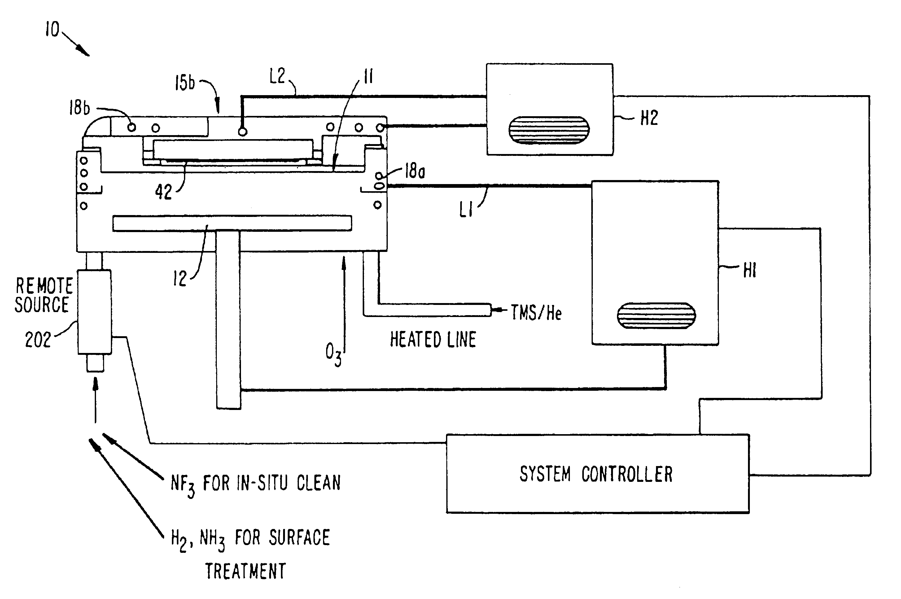
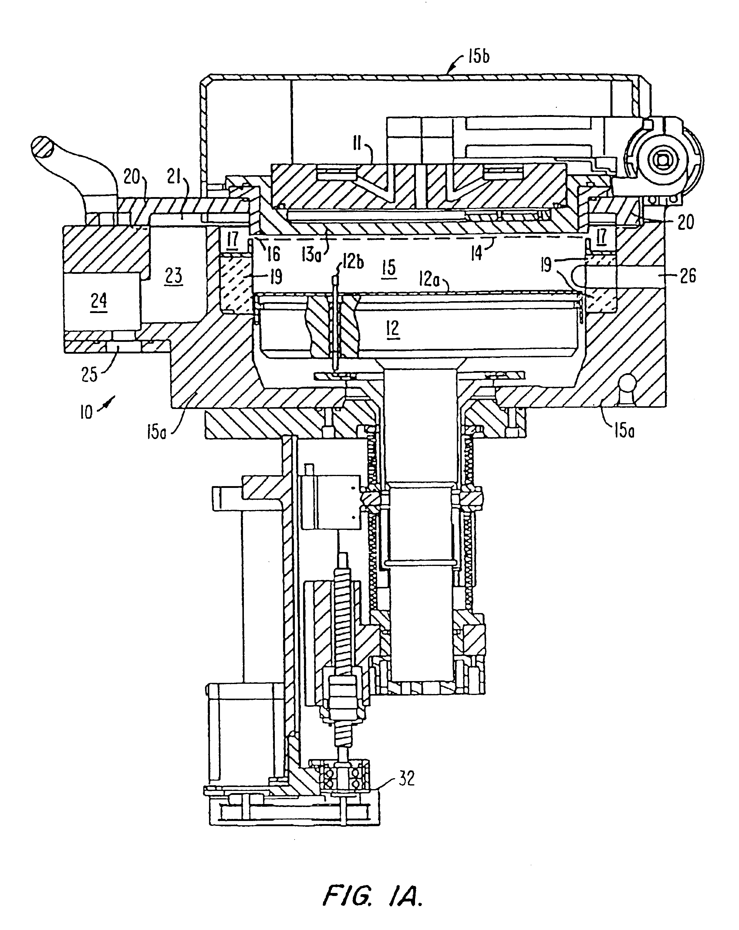
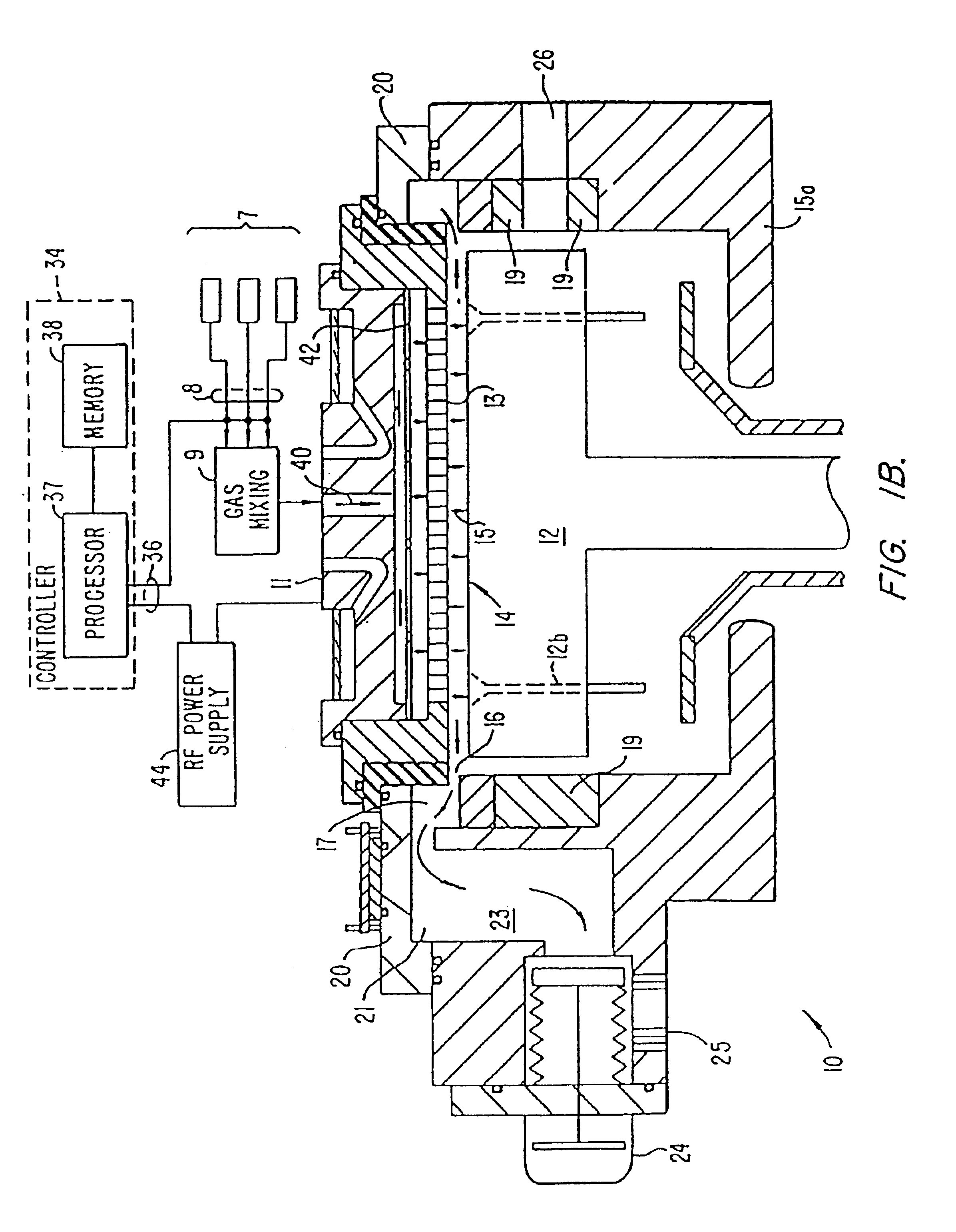
[0032]One suitable CVD apparatus in which the method of the present invention can be carried out is shown in FIGS. 1A and 1B, which are vertical, cross-sectional views of a CVD system 10, having a vacuum or processing chamber 15 that includes a chamber wall 15a and chamber lid assembly 15b. Chamber wall 15a and chamber lid assembly 15b are shown in exploded, perspective views in FIGS. 1C and 1D.
[0033]CVD system 10 contains a gas distribution manifold 11 for dispersing process gases to a substrate (not shown) that rests on a heated pedestal 12 centered within the process chamber. During processing, the substrate (e.g. a semiconductor wafer) is positioned on a flat (or slightly convex) surface 12a of pedestal 12. The pedestal can be moved controllably between a lower loading / off-loading position (depicted in FIG. 1A) and an upper processing position (indicated by dashed line 14 in FIG. 1A and shown in FIG. 1B), which is closely adjacent to manifold 11. A centerb...
PUM
| Property | Measurement | Unit |
|---|---|---|
| Temperature | aaaaa | aaaaa |
| Temperature | aaaaa | aaaaa |
| Temperature | aaaaa | aaaaa |
Abstract
Description
Claims
Application Information


