Nitride semiconductor laser diode

a laser diode and semiconductor technology, applied in semiconductor lasers, laser details, electrical equipment, etc., can solve the problems of inability to realize practical use, increase the cost of production, and the inability to directly emit green beams, so as to improve the life characteristics and excellent light emission efficiency and life properties.

Active Publication Date: 2012-07-26
NICHIA CORP
View PDF7 Cites 24 Cited by
  • Summary
  • Abstract
  • Description
  • Claims
  • Application Information

AI Technical Summary

Benefits of technology

[0025]As described above, according to the present invention, in a nitride semiconductor laser diode of lasing wavelength 500 nm or greater, occurrence of the dislocations originating from the light emitting layer with an increase in the In content is intentionally left in situ. Thus, while favorably maintaining the carrier confinement in the InGaN light emitting layer and the crystal quality thereof, the concentration of p-type impurity present within a predetermined distance from the InGaN light emitting layer is controlled in a predetermined range, and thus exponential improvement in the life characteristics can be achieved. Accordingly, a long wavelength nitride semiconductor laser diode with excellent light emitting efficiency and life properties can be realized.

Problems solved by technology

However, a direct green laser diode capable of directly emitting a green beam has not yet been put into practical use.
As for a semiconductor laser diode capable of directly emitting green light, a laser diode using a Group II-VI compound semiconductor was reported around 1993, but because of its poor reliability at high current condition, its practical use was not realized.
However, in the case where the InGaN light emitting layer is grown by vapor phase epitaxy, the lattice mismatch with respect to GaN layer which is an underlayer thereof, becomes greater with increase of In content, and InGaN layer itself becomes chemically unstable and phase separation tends to occur.
For this reason, the realization of a semiconductor laser capable of emitting green light, by way of increasing the In content in the InGaN light emitting layer is not easy.

Method used


Image

  • Nitride semiconductor laser diode
  • Nitride semiconductor laser diode
  • Nitride semiconductor laser diode

Examples


example 1

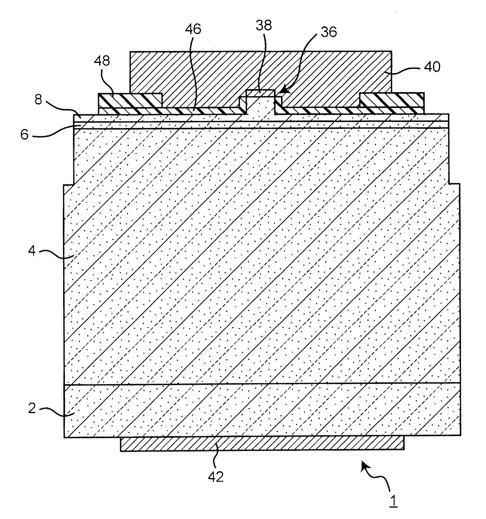
[0093]A nitride semiconductor laser having a structure shown in FIG. 1 is manufactured as described below.

(N-Side Nitride Semiconductor Layer 4)

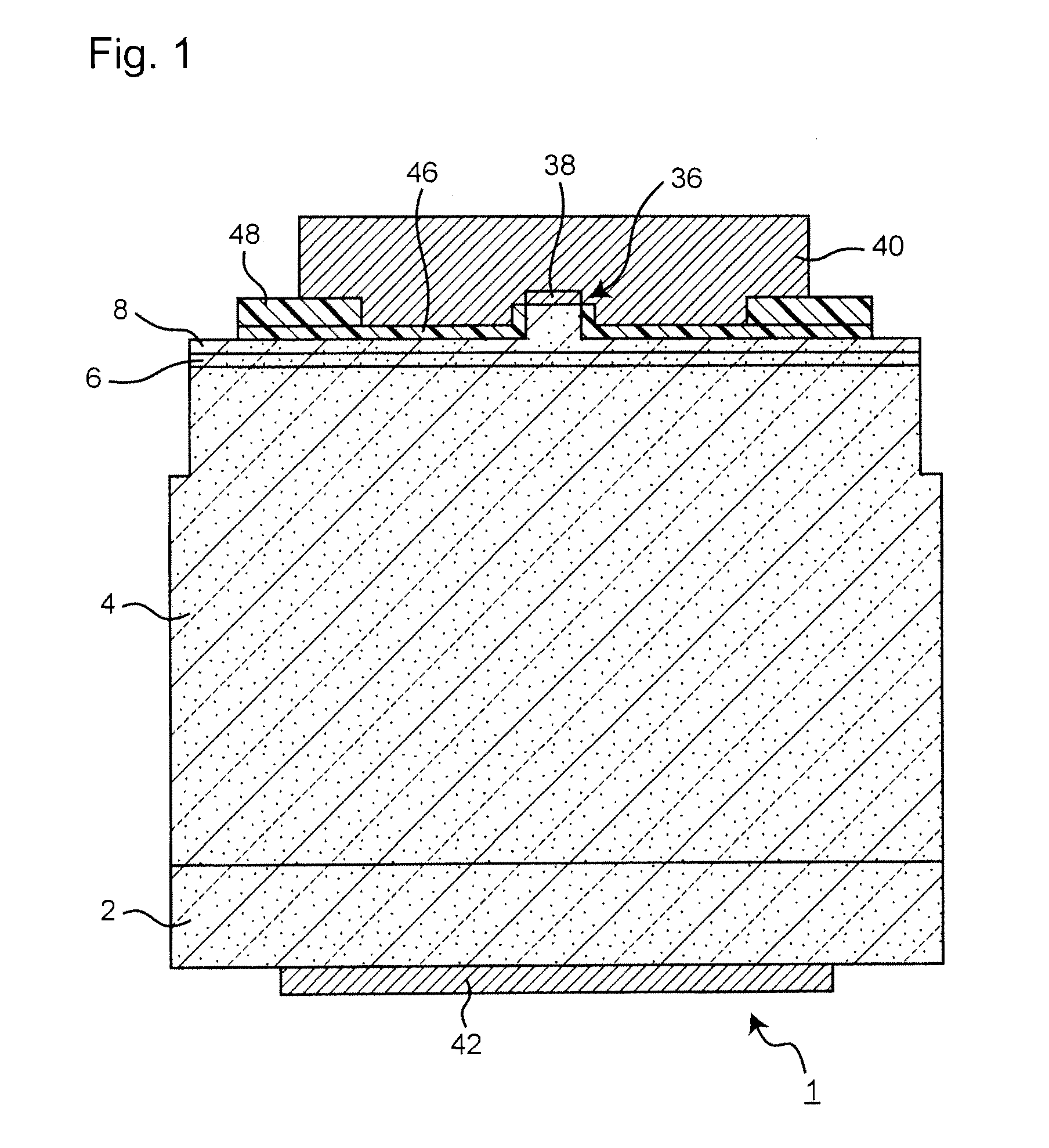
[0094]First, a gallium nitride substrate 2, which has a C-plane as a principal surface, with dislocation density of about 5×105 cm−2 is prepared. Then, an n-type Al0.03Ga0.97N layer 12 doped with Si at 3×1018 cm3 is grown to a thickness of 2 m (first n-side nitride semiconductor layer) by using TMG (trimethyl gallium, TMA (trimethyl aluminum), SiH4 (silane), and ammonia at 1140° C. with hydrogen as carrier gas by using MOCVD on the gallium nitride substrate 2. Following that, at the temperature of 930° C. and using TMI (trimethyl indium), an n-type In0.06Ga0.94N layer 14 doped with Si at 4×1015 cm3 is grown to a thickness of 0.15 m (second n-side nitride semiconductor layer). Next, at the temperature of 990° C., an n-type Al0.09Ga0.91N layer 16 doped with Si at 2×1018 cm3 is grown to a thickness of 1 m (third n-side nitride semiconductor lay...

example 2

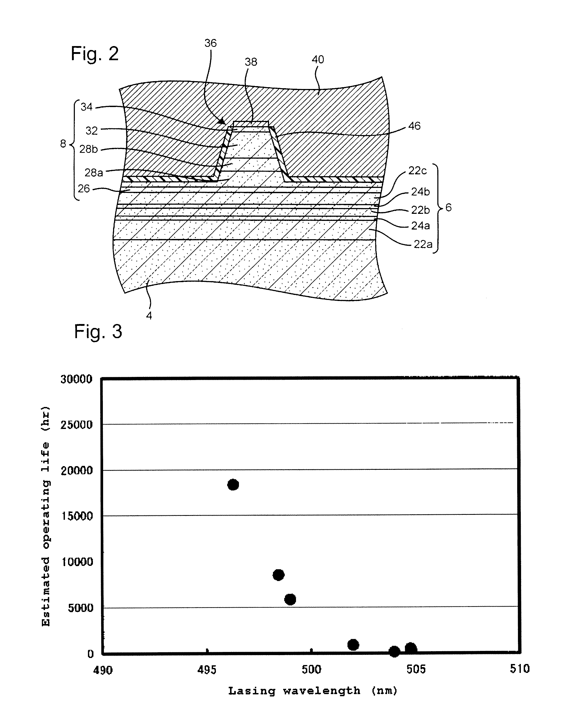
[0105]In Example 1, the composition of the well layer is In0.25Ga0.73N, with a thickness of 2.5 nm, and the number of the well layers is 3. The concentration of Mg incorporated in the p-type Al0.2Ga0.8N layer 26 (first p-type nitride semiconductor layer) is 2×1019 cm−3, the concentration of Mg incorporated in the p-type Al0.03Ga0.97N layers 28a, 28b (second p-type nitride semiconductor layer) is 2×1018 cm−3, 4×1018 cm−3 respectively. The nitride semiconductor laser is manufactured in the same manner as in Example 1 except for that described above. Dislocations of about 5×106 cm−2 occur from the active layer 6. The lasing wavelength is 517 nm, the threshold current is 70 mA, and output is 5 mW. Life test at 60 C., APC, and 5 mW shows an estimated operating life is 10,000 hours or greater.

example 3

[0106]In Example 1, the composition of the well layer is In0.27Ga0.73N, with a thickness of 2.2 nm, and the number of the well layers is 4. The concentration of Mg incorporated in the p-type Al0.2Ga0.8N layer 26 (first p-type nitride semiconductor layer) is 3×1019 cm−3, the concentration of Mg incorporated in the p-type Al0.03Ga0.97N layers 28a, 28b (second p-type nitride semiconductor layer) is 3×1018 cm−3, 6×1018 cm−3 respectively. The nitride semiconductor laser is manufactured in the same manner as in Example 1 except for that described above. Dislocations of about 7.5×106 cm−2 occur from the active layer 6. Lasing occurs at 540 nm, and a life test at 60° C., APC, and 5 mW shows a significantly preferable operating life characteristics compared to that of Comparative Example.


PUM

PropertyMeasurementUnit
lasing wavelengthaaaaaaaaaa
thicknessaaaaaaaaaa
thicknessaaaaaaaaaa

Abstract

A nitride semiconductor laser diode includes a substrate, an n-side nitride semiconductor layer formed on the substrate, an active layer formed on the n-side nitride semiconductor layer and having a light emitting layer including InxAlyGa1−x−yN (0<x<1, 0 y<1, 0<x+y<1), and a p-side nitride semiconductor layer formed on the active layer. In the nitride semiconductor laser diode, the lasing wavelength of the nitride semiconductor laser diode is 500 nm or greater, dislocations originated in the active layer penetrate through the p-side nitride semiconductor layer, with the dislocation density in the p-side nitride semiconductor layer being 1×106 cm−2 or greater, and the concentration distribution of p-type impuritys in the depth direction is such that, from the light emitting layer toward the surface of the p-side nitride semiconductor layer, the concentration of the p-type impurity reaches a maximum value of 5×1018 cm−3 or greater within a range of 300 nm from the top portion of the light emitting layer which is closest to the p-side nitride semiconductor layer, and after reaching the maximum value, the concentration remains at 6×1017 cm−3 or greater in the above-described range of 300 nm.

Description

BACKGROUND OF THE INVENTION[0001]1. Field of the Invention[0002]The present invention relates to a nitride semiconductor laser diode using a nitride semiconductor represented by AlxInyGa1−x−N (0 x 1, 0 y 1, 0 x+y 1).[0003]2. Description of Related Art[0004]A semiconductor laser diode using a compound semiconductor is widely used in applications such as optical disc systems capable of recording and / or reproducing large volume, high-density information. Meanwhile, a new application for semiconductor laser diodes which will provide a full color display with a combination of blue, green, and red semiconductor lasers is expected to be realized.[0005]Among blue, green, and red of the three principal colors of light, blue and red semiconductor laser diodes are already in practical use with employing Group III-V compound semiconductors such as InAlGaN and AlInGaP. In contrast, as for a green laser, a laser device capable of emitting a green beam has been developed by converting wavelength u...

Claims


Application Information

Patent Timeline
Patent Type & Authority Applications(United States)
IPC IPC(8): H01S5/34H01S5/323
CPCB82Y20/00H01S5/22H01S5/34333H01S5/34H01S5/3063H01S5/3013H01S5/0021H01S5/3068
Inventor MIYOSHI, TAKASHI
Owner NICHIA CORP
Why Eureka
Try Eureka