Semiconductor device and manufacturing method therefor

a technology of semiconductor devices and semiconductors, applied in semiconductor devices, semiconductor/solid-state device details, capacitors, etc., can solve the problems of reducing ion energy, difficult to secure an adequate area for electrodes in the dram, and difficulty in dry etching to form capacitor holes, etc., to achieve high stability, increase the strength of the base-side and top-side, and high aspect ratio

Inactive Publication Date: 2009-06-04
ELPIDA MEMORY INC
View PDF3 Cites 11 Cited by
  • Summary
  • Abstract
  • Description
  • Claims
  • Application Information

AI Technical Summary

Benefits of technology

[0021]Due to the double processing, it is possible to form a large capacitor hole having a high aspect ratio and a high stability. It is possible to increase the strengths of the base-side and top-side lower electrode films by the remaining portion of the metal plug which remains due to partial etching; thus, it is possible to form the capacitor having high strengths of electrodes.
[0022]In result, it is possible to control the aspect ratio of the capacitor hole from being excessively increased in manufacturing; and it is possible to increase the capacitive electrode area in the semiconductor device.

Problems solved by technology

Due to recent progresses for further refining the structures of semiconductors, it becomes difficult to secure an adequate area for electrodes in the DRAM.
Refining the structure of the DRAM increases the effective aspect ratios of capacitor holes and makes it difficult to perform dry etching to form capacitor holes.
When effective aspect ratios becomes extremely high, they speed up a reduction of ion energy and a reduction of the etching speed, thus eventually causing an etch-stop event in which etching reaction stops progressing.

Method used


Image

  • Semiconductor device and manufacturing method therefor
  • Semiconductor device and manufacturing method therefor
  • Semiconductor device and manufacturing method therefor

Examples


Embodiment Construction

[0039]The present invention will now be described herein with reference to illustrative embodiments. Those skilled in the art will recognize that many alternative embodiments can be accomplished using the teachings of the present invention and that the invention is not limited to the embodiments illustrated for explanatory purposes.

[0040]The illustrations are used to explain a semiconductor device and its manufacturing method in accordance with the present invention; hence, the sizes, thicknesses, and dimensions regarding layers, films, and components do not necessarily match the sizes, thicknesses, and dimensions of actual products of semiconductor devices.

1. Manufacturing Method

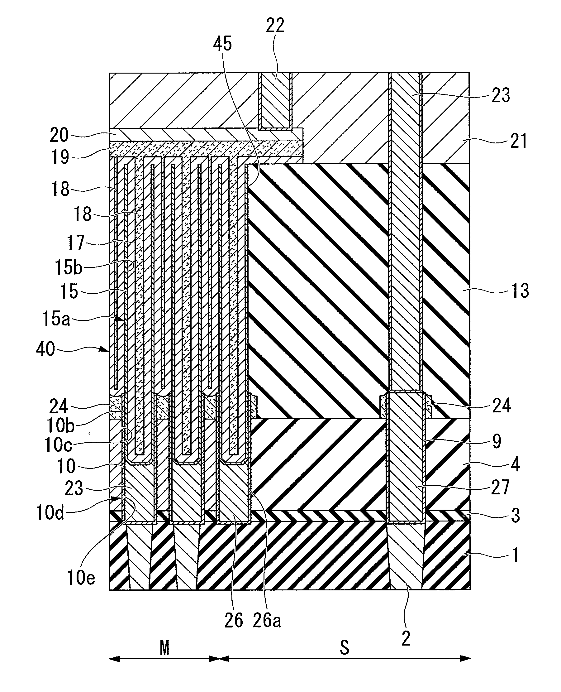
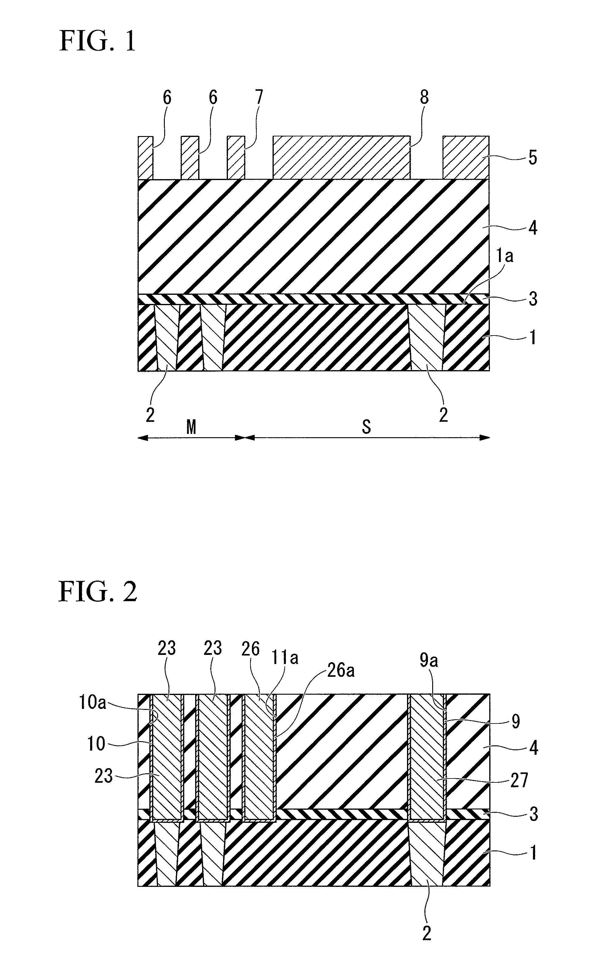
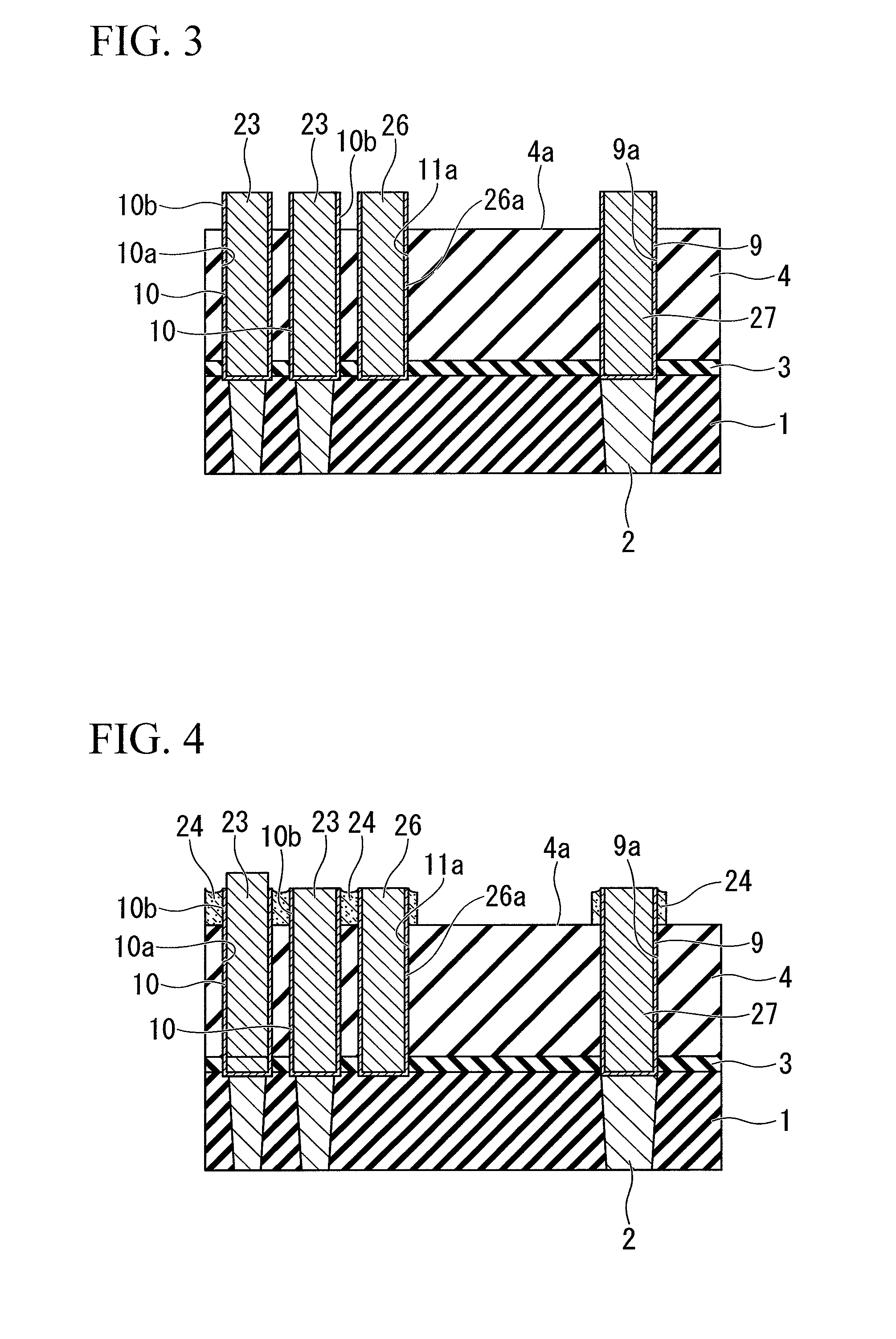
[0041]A manufacturing method of a semiconductor device according to one embodiment of the present invention will be described with reference to FIGS. 1 to 12.

[0042]The manufacturing method of the semiconductor device of the present embodiment includes a first step for forming a first sacrifice insulating fi...


PUM


Abstract

A semiconductor device includes capacitors formed on the surface of an interlayer insulating film in connection with capacitive contact plug, wherein capacitors are constituted of base-side lower electrode films having hollow-pillar shapes, metal plugs embedded in hollows of base-side lower electrode films, and top-side lower electrode films having hollow-pillar shapes engaged with the upper portions of the hollows as well as dielectric films and upper electrode films which are sequentially laminated so as to cover the peripheral surfaces of the base-side and top-side lower electrode films and the interior surfaces of the top-side lower electrode films. Side walls are further formed to connect together the adjacent base-side lower electrode films. Thus, it is possible to control the aspect ratio of a capacitor hole for embedding the metal plug from being excessively increased, and it is possible to increase the capacitive electrode area of each capacitor.

Description

BACKGROUND OF THE INVENTION[0001]1. Field of the Invention[0002]The present invention relates to semiconductor devices including memory cells such as dynamic random-access memories and manufacturing methods therefor.[0003]The present application claims priority on Japanese Patent Application No. 2007-312823, the content of which is incorporated herein by reference.[0004]2. Description of Related Art[0005]Various technologies regarding semiconductor devices including dynamic random-access memories have been developed and disclosed in various documents such as Patent Documents 1-3.[0006]Patent Document 1: Japanese Unexamined Patent Application Publication No. H11-204753[0007]Patent Document 2: Japanese Unexamined Patent Application Publication No. 2006-324363[0008]Patent Document 3: Japanese Unexamined Patent Application Publication No. 2007-81189[0009]A typical example of a dynamic random-access memory (DRAM) includes a plurality of memory cells which are constituted of transistors a...

Claims


Application Information

Patent Timeline
Patent Type & Authority Applications(United States)
IPC IPC(8): H01L23/48
CPCH01L21/76834H01L21/76885H01L28/91H01L27/10894H01L27/10852H10B12/033H10B12/09
Inventor SUKEKAWA, MITSUNARI
Owner ELPIDA MEMORY INC
Why Eureka
Try Eureka