High density inductor and method for producing same

a high-density inductor and high-density technology, applied in the field of high-density inductor, can solve the problems of limiting the downsizing and thickness reduction of the above-described inductor, the inability to reduce the space between the wires of the coil, and the inability to form a deep vertical pattern

Inactive Publication Date: 2004-08-26
TDK CORPARATION
View PDF8 Cites 94 Cited by
  • Summary
  • Abstract
  • Description
  • Claims
  • Application Information

AI Technical Summary

Benefits of technology

[0036] According to the above-described features of the present invention, since a thin film formation process is used to shape a coil, the coil can be made compact and shaped precisely. Consequently, the size of a core member enveloping the coil can also be reduced. Thus, the inductor itself can be made compact.
[0037] According to the invention, the coil has a structure in which a plurality of wire layers are piled up, wherein the ratio of the thickness to the wire width or the aspect ratio of each wire layer is designed to be low. In the case that each wire layer is formed by a thin film formation process, it is possible to prevent resist in which a groove portion has been formed from bending or collapsing by setting the aspect ratio as low as a value with which collapse or detachment of the resist is hard to occur. Therefore, it is possible to form a wire layer reliably. Thus, a coil with a large thickness dimension or a high aspect ratio can be eventually formed by repeating the thin film formation process to pile up the wire layers each of which has a low aspect ratio.

Problems solved by technology

There is a limit to the downsizing and thickness reduction of the above-described inductor, since its production process includes a mechanical operation of wrapping the electroconductive member around the core.
However, the above-mentioned coils formed by a thin film technology or the above-mentioned methods of forming a coil utilizing natural growth by plating suffer from the following problems.
This causes another problem, that is, the coil pattern cannot be formed deeply in the vertical direction.
As a result, it is impossible to reduce the space between the wires of the coil.)
Consequently, it is not possible to increase the substrate surface density, and therefore it is not possible to increase productivity.
In addition, use of a material that are hard to be processed, such as a ferrite, for the substrate causes an increase in cost.
Consequently, the ratio of the cross sectional area of the sheet to the cross sectional area of the coil becomes large, so that the occupation density of the coil in the interior of the inductor is unfavorably decreased.
However, since the deposit member 12 is formed by natural growth, it is not possible to increase the aspect ratio of the coil to more than 1.
Consequently, the ratio of the cross sectional area of the sheet to the cross sectional area of the coil becomes large, so that the occupation density of the coil in the interior of the inductor is unfavorably decreased.
In the process disclosed in Japanese Patent Application Laid-Open No. 2001-102235, there is the risk that a pattern can be bent or removed or the depth of focus at the exposure wavelength can be narrowed like in the case of the above-described coil produced by utilizing a thin film technology.
However, since the overlapping coils are only a pair of coils, it is difficult for this process also to attain the aspect ratio that can be realized by the present invention.

Method used


Image

  • High density inductor and method for producing same
  • High density inductor and method for producing same
  • High density inductor and method for producing same

Examples


Embodiment Construction

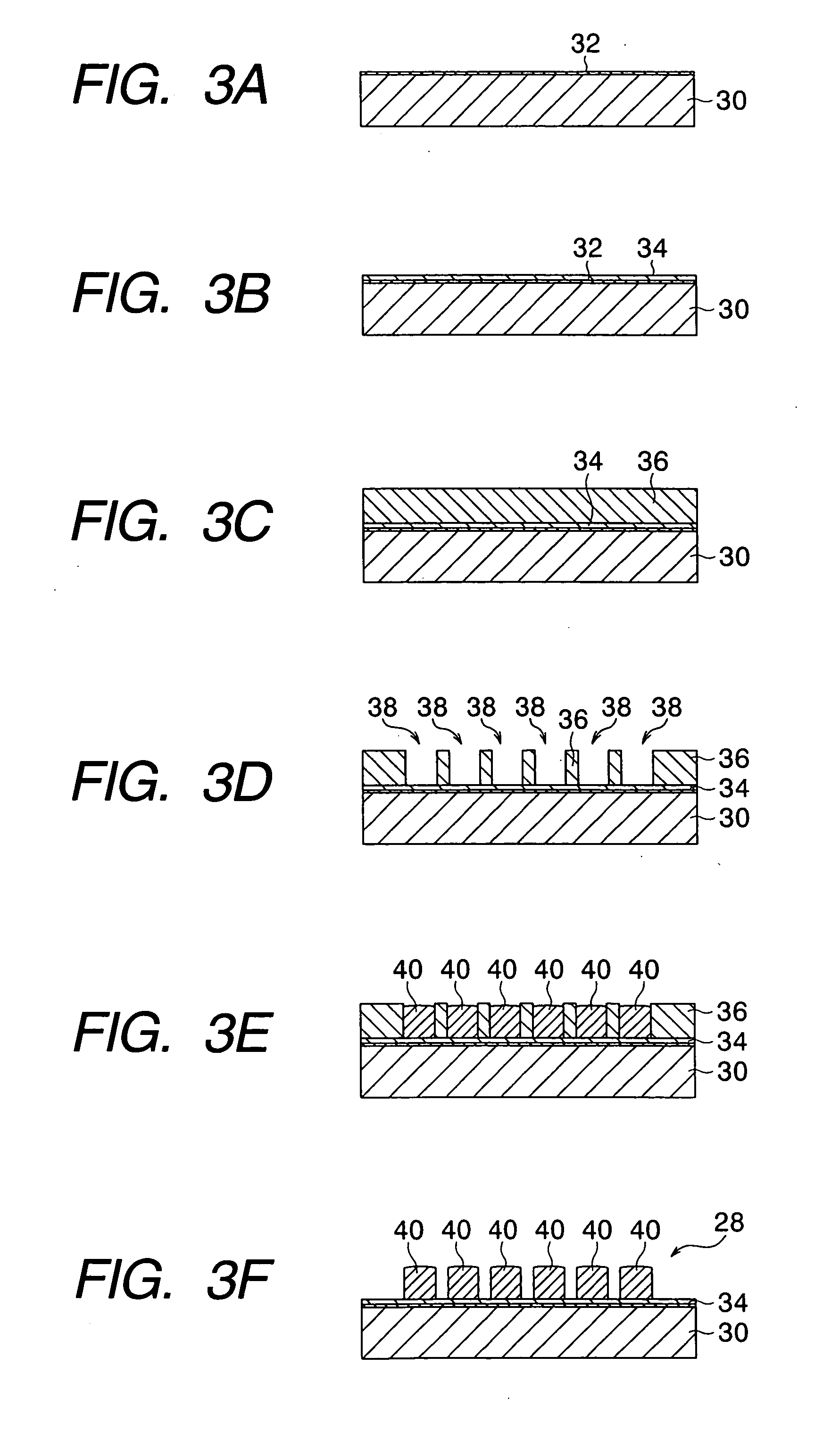
[0121] A coil pattern was formed on a substrate having a base conductive layer. For example in the case that a coil pattern with a thickness of the electroconductive portion of 40 .mu.m and a width of the coil interval space of 10 .mu.m is to be formed, the width of the resist pattern should be 10 .mu.m. The allowable height for the resist of the aforementioned width with which the width of the resist will remain constant and the resist will not be bent is about 40 .mu.m or less. In order to ensure the resolution realizing a resist width of 10.+-.2 .mu.m in both the upper and lower portions of the pattern, exposure light having a wavelength of 360 nm was used.

[0122] With the above conditions, the first layer of the coils with the coil width of 40 .mu.m and a spacing of 10 .mu.m was formed.

[0123] At that time, all of the coils of the first layer were normally formed on the substrate without being bent, in other words the process yield was 100%.

[0124] Next, a pattern of the second lay...


PUM

PropertyMeasurementUnit
heightaaaaaaaaaa
heightaaaaaaaaaa
thicknessaaaaaaaaaa

Abstract

A method for producing a high density inductor includes the steps of forming a coil having a spiral shape, sealing the coil in the interior of a core member, and forming a terminal electrode for allowing electric conduction to said coil on the outside of said core member. In this method, the coil is formed by repeating a process of forming a wire layer by means of a thin film forming process and a process of forming an additional wire layer on top of the wire layer by means of the thin film forming process to pile up the wire layers. With this production method, it is possible to form a coil with a high aspect ratio. In addition, the inductor is designed in such a way that the core member envelopes only the coil. With that design, it is possible to make the inductor compact.

Description

[0001] 1. Field of the Invention[0002] The present invention relates to an inductor for use in an electronic circuit and a method for producing the same. More specifically, the present invention relates to a high density inductor that is reduced in size to allow high density mounting on a substrate and a method of producing such a high density inductor.[0003] 2. Related Background Art[0004] An inductor as an electronic part has the property of storing current energy. Inductors are used in DC-DC converters, switching power sources and other devices and equipped in various electronic apparatuses.[0005] In recent years, with downsizing and thickness reduction of electronic apparatuses such as cellular phones and personal digital assistants (PDAs), downsizing and thickness reduction of inductors have been demanded.[0006] In the following, the structure and production method of conventional inductors will be described.[0007] FIGS. 7A and 7B are perspective views showing inductors accordi...

Claims


Application Information

Patent Timeline
Patent Type & Authority Applications(United States)
IPC IPC(8): H01F17/00H01F17/04H01F27/32H01F37/00H01F41/04H01L27/08H05K1/16H05K3/10H05K3/24
CPCH01F17/0013H01F27/323H01F41/042H01F41/046H05K2203/1476H05K1/165H05K3/108H05K3/244H05K2203/0577H01L27/08
Inventor SHOJI, SHIGERU
Owner TDK CORPARATION
Why Eureka
Try Eureka