

Method, device and chip for reducing core size of nonvolatile flash memory
A non-volatile, flash memory technology, applied in the direction of instruments, electrical digital data processing, electrical components, etc., can solve problems affecting device performance, reduce the overall area, avoid the increase of leakage current, and reduce the core size.
- Summary
- Abstract
- Description
- Claims
- Application Information
AI Technical Summary
Problems solved by technology
Method used
Image

Examples
Embodiment Construction
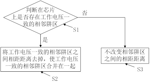
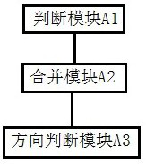
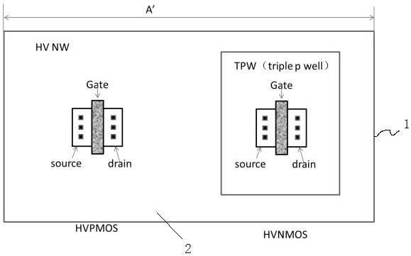
[0029] The following will clearly and completely describe the technical solutions in the embodiments of the present application with reference to the accompanying drawings in the embodiments of the present application. Obviously, the described embodiments are only some of the embodiments of the present application, not all of them. The components of the embodiments of the application generally described and illustrated in the figures herein may be arranged and designed in a variety of different configurations. Accordingly, the following detailed description of the embodiments of the application provided in the accompanying drawings is not intended to limit the scope of the claimed application, but merely represents selected embodiments of the application. Based on the embodiments of the present application, all other embodiments obtained by those skilled in the art without making creative efforts belong to the scope of protection of the present application.
[0030] It should ...
PUM
 Abstract
Description
Claims
Application Information