

Defect controlled nanotube sensor and method of production
a nanotube sensor and control technology, applied in the field of nanotubes, to achieve the effect of preventing light exposure and high defect density
- Summary
- Abstract
- Description
- Claims
- Application Information
AI Technical Summary
Benefits of technology
Problems solved by technology
Method used
Image

Examples
example 1
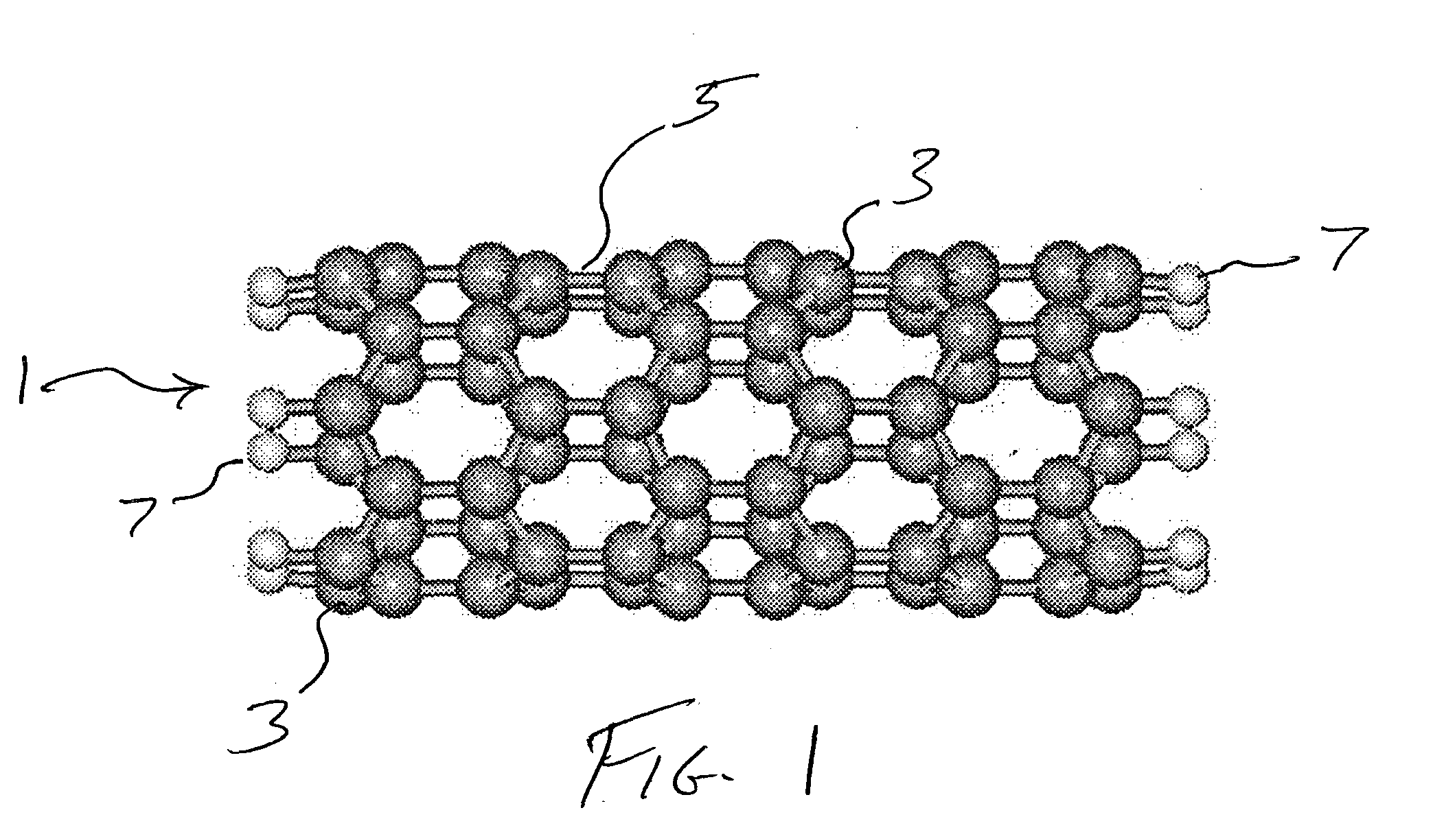
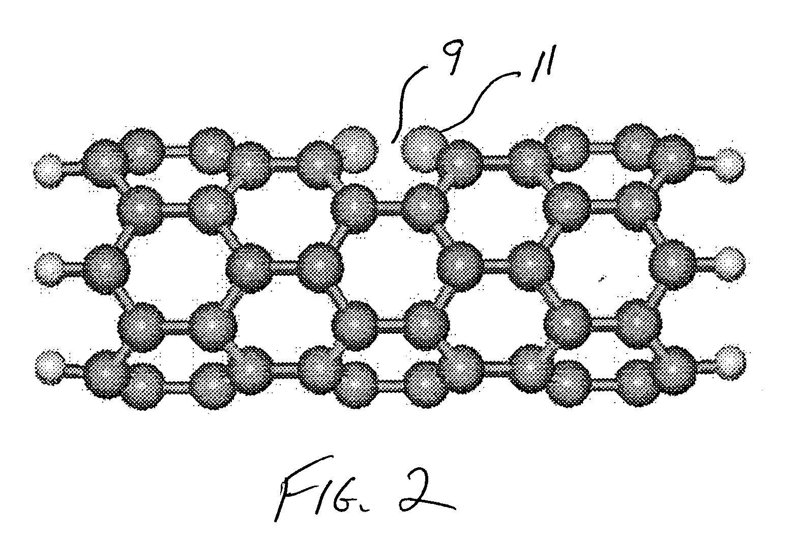
[0172] Nanotube models are based upon nanotubes about 1 nm long, and diameters of about 0.5 nm. The models are relatively small as compared to average actual carbon nanotubes but are representative. Computing power needed for atomic level simulations grows very rapidly with the number of atoms, therefore there are limitations with regard to the size of the model.
[0173] Nanotube simulations are carried out by using a software called HyperChem, from HyperCube; Inc, Gainesville, Fla., which is a typical molecular modeling software used in Quantum Chemistry. HyperChem includes a graphical user interface which is used to draw the model. Atoms forming the backbone of the nanotube are entered by mouse clicks. Typically, one would enter the nanotube as a 2 dimensional planar object, then joins the ends that roll into a tube and finally use the model building feature of the software to adjust the bond lengths and bond angles. It is generally recommended to further optimize the geometry by u...
example 2
[0176] Defects can be introduced into semiconductive and conductive carbon nanotubes, and a simulation of introducing defects can be prepared by modifying the models of carbon nanotubes without defects.
[0177] In order to simulate a broken carbon-carbon bond of a carbon nanotube, a bond of a 6-membered ring was broken at one location and hydrogen is attached to the dangling bonds. After introducing the defect, Molecular Mechanics method is used to optimize the geometry around the defect.
[0178] Results:
Semiconductive nanotubeNo defectWith defectChangeBandgap3.84eV3.77eV −2%Axial polarizability2300au2660au+16%Radial polarizability1670au1980au+19%Conductive nanotubeBandgap2.07eV2.65eV+28%Axial polarizability3530au4020au+14%Radial polarizability1650au1710au +4%
[0179] Defects especially change the properties of the conductive nanotube and the bandgap becomes bigger (conductance decreases). As discussed above, it is also possible to introduce defects during the growth process of the na...
example 3
[0180] Recently it has been noted that the bandgap of boron nitride nanotube varies with electric field, and similar results have been observed during simulations with carbon nanotubes. Therefore, this example is a simulation in more detail of the variation of bandgap as a function of the applied electric field.
[0181] Semiconductive nanotubes (diameter: 0.4 nm, length: 1.1 nm, number of 6 member rings included in the circumference: 5) and conductive nanotube (diameter: 0.5 nm, length: 1.1 nm, number of 6 member rings included in the circumference: 6) are used in this stimulation. An electric field is applied along the axial direction and the diameter direction and allowed energy levels and bandgap are calculated. Simulation results are shown in FIG. 15.
[0182] Results are as follows: [0183] The bandgap of both types of nanotubes varies considerably with electric field; the magnitude of variation reaches several eV. [0184] With increasing electric field, the bandgap of semiconductiv...
PUM
 Abstract
Description
Claims
Application Information