Method of fabricating a microfabricated high aspect ratio device with electrical isolation

a microfabricated device and high aspect ratio technology, applied in the field of microfabricated devices, can solve the problems of significant fabrication difficulties, inability to achieve fabrication techniques, and inability to wire bond structural elements to electronics, etc., to achieve increased signal-to-noise ratio, high vertical aspect ratio, and large sense capacitance

Inactive Publication Date: 2005-11-01
RGT UNIV OF CALIFORNIA
View PDF28 Cites 99 Cited by
  • Summary
  • Abstract
  • Description
  • Claims
  • Application Information

AI Technical Summary

Benefits of technology

[0014]Advantages of the invention include the following. The microstructures are electrically isolated from the microelectronic circuits, but can be electrically connected to the microelectronic circuits by interconnect layers. The device may be fabricated utilizing standard microfabrication techniques. The invention is compatible with existing very large scale integrated (VLSI) circuit fabrication processes so that microelectronic circuits may be fabricated on the surface of the device. The microstructures have a high vertical aspect ratio (on the order of 10:1 to 25:1 or even higher). Microsensors fabricated according the invention have a larger sense capacitance, and thus an increased signal-to-noise ratio, due to the increased surface area between the electrode fingers. The microstructures also have a larger mass and a larger moment of inertia, and consequently thermal noise is reduced. In addition, the high vertical aspect ratio microstructures have a large separation of vibrational modes.

Problems solved by technology

Several techniques have been developed for making is high aspect ratio microstructures, but these techniques have significant fabrication difficulties.
One problem in some existing techniques is that the structural elements need to be wire bonded to the electronics.
Because differential capacitance-based sensors may require the interconnection of many alternating positive and negative electrode plates (e.g., one hundred plates in an angular accelerometer), the large number of wire bonds makes this fabrication technique impractical.
Another problem in some existing techniques is difficulty in electrically isolating the microstructure elements from each other and from the microelectronic circuits on the chip.
Consequently, capacitive sensing schemes cannot be implemented easily using existing techniques.

Method used


Image

  • Method of fabricating a microfabricated high aspect ratio device with electrical isolation
  • Method of fabricating a microfabricated high aspect ratio device with electrical isolation
  • Method of fabricating a microfabricated high aspect ratio device with electrical isolation

Examples


Embodiment Construction

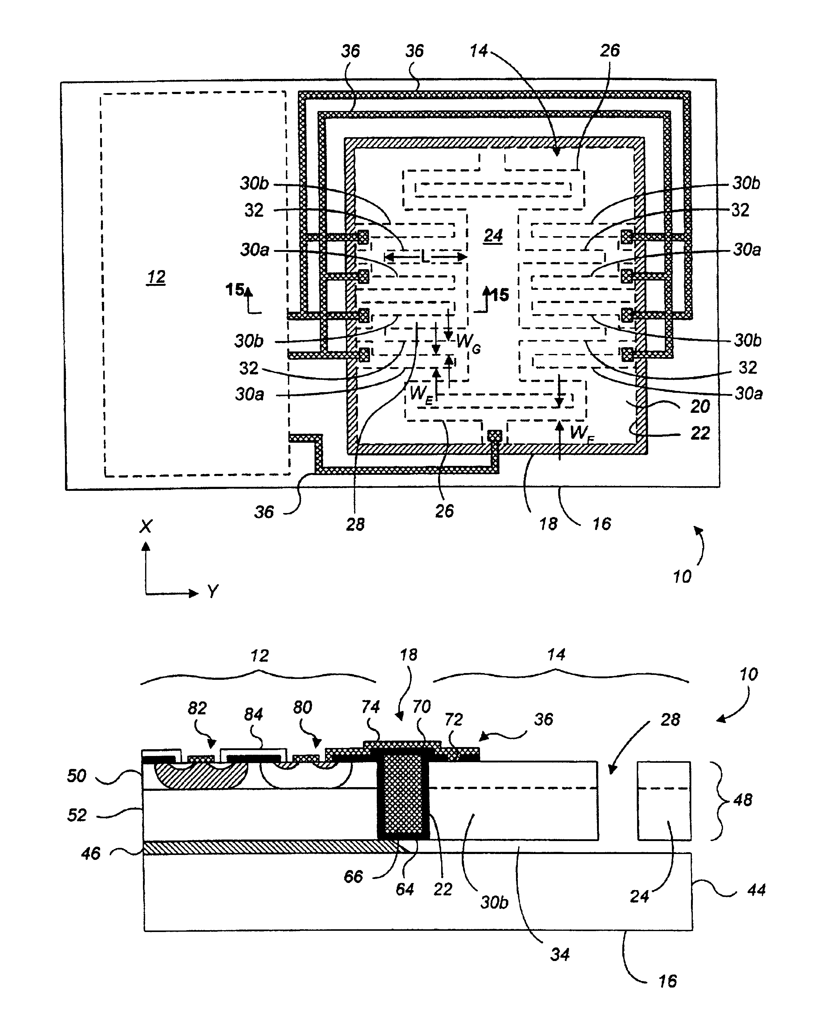
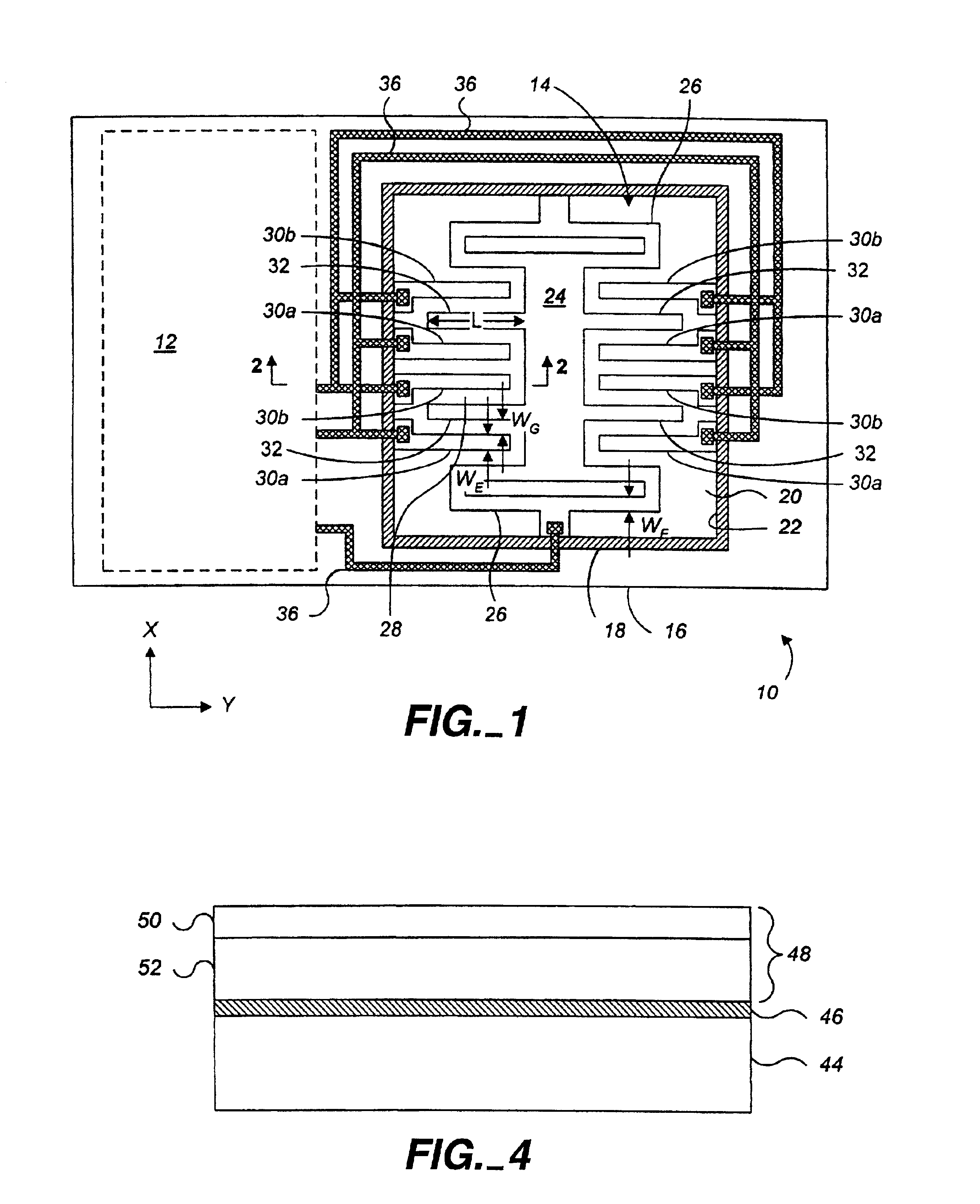
[0026]FIGS. 1, 2 and 3 illustrate a microfabricated device 10 in accordance with the present invention. The illustrated microfabricated device is a linear accelerometer. However, the principles of the invention are applicable to many other devices, such as vibromotors, angular accelerometers, gyroscopes, resonators, microactuators, microvalves, filters, and chemical detectors.

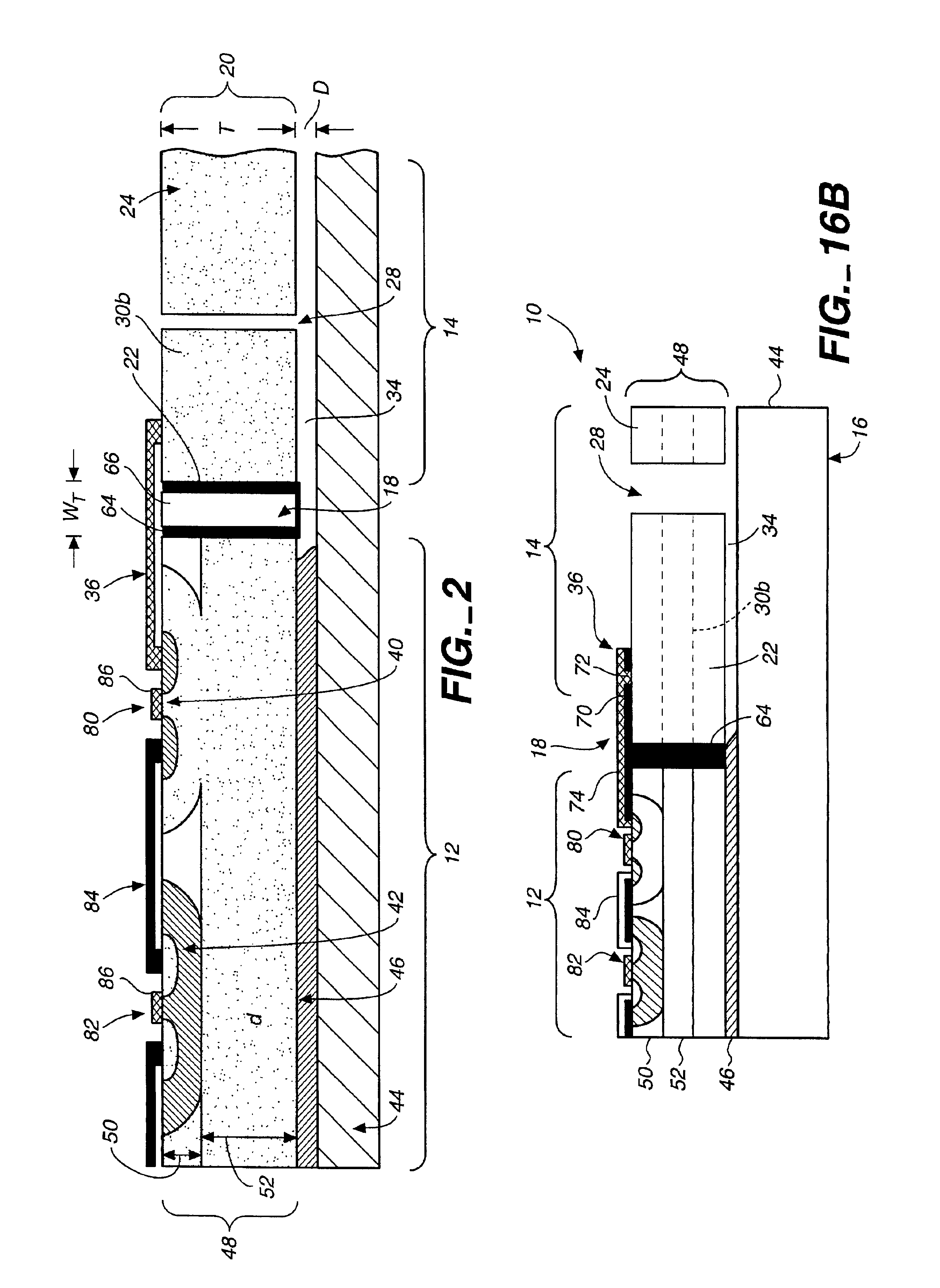
[0027]Device 10 includes a circuit region 12 and a structure region 14 formed in a substrate 16. As will be described in more detail below, microstructure elements in structure region 14 are electrically isolated from each other and from circuit region 12 by a filled isolation trench region 18.

[0028]A recess 20 is etched into an upper surface of substrate 16 in structure region. Recess 20 contains the various microstructure elements, such as electrodes fingers and plates, flexures, and proof mass beams or bodies, required by device 10. The microstructure elements in recess 20 are defined and separated by a chan...


PUM


Abstract

A microfabricated device having a high vertical aspect ratio and electrical isolation between a structure region and a circuit region. The device may be fabricated on a single substrate and may include electrical interconnections between the structure region and the circuit region. The device includes a substrate and an isolation trench surrounding a structure region in the substrate. The isolation trench includes a lining of a dielectric insulative material. A plurality of microstructure elements are located in the structure region and are laterally anchored to the isolation trench.

Description

[0001]This is a division of U.S. application Ser. No. 08 / 874,568, filed Jun. 13, 1997 now U.S. Pat. No. 6,121,552.STATEMENT OF GOVERNMENT RIGHTS[0002]This invention was made with Government support under Grant (Contract) Nos. DABT63-93-C-0065 and DABT63-95C-0028 awarded by DARPA. The Government has certain rights to this invention.BACKGROUND OF THE INVENTION[0003]The present invention relates generally to microfabricated devices, and more particularly to three dimensional microfabricated devices having a high vertical aspect ratio.[0004]Microelectromechanical systems (MEMS) integrate micromechanical structures and microelectronic circuits on the same silicon chip to create an integrated device. MEMS have many useful applications such as microsensors and microactuators. An example of a microsensor is a gyroscope used in a missile guidance system. An example of a microactuator is a micropositioner used to move a read / write head in a disk drive.[0005]In surface micromachining, the devi...

Claims


Application Information

Patent Timeline
Patent Type & Authority Patents(United States)
IPC IPC(8): B81B3/00B81B7/00B81B7/02G01P15/10G01P15/097G01P15/08G01C19/56G01P15/125G01C19/5719
CPCB81C1/00246G01C19/5719G01P15/0802G01P15/0888G01P15/097G01P15/125B81B2203/033B81C2203/0778G01P2015/0814
Inventor BROSNIHAN, TIMOTHY J.BUSTILLO, JAMESCLARK, WILLIAM A.
Owner RGT UNIV OF CALIFORNIA
Why Eureka
Try Eureka