Low capacitance junction-isolation for bulk FinFET technology

a technology of low capacitance and junction isolation, which is applied in the direction of semiconductor devices, basic electric elements, electrical apparatus, etc., can solve the problems of expensive source/drain isolation schemes in prior art methods, and achieve the effect of good junction isolation and low capacitance benefits of finfets

Active Publication Date: 2006-09-05
GLOBALFOUNDRIES US INC
View PDF13 Cites 393 Cited by
  • Summary
  • Abstract
  • Description
  • Claims
  • Application Information

AI Technical Summary

Benefits of technology

[0008]The present invention provides a SiGe-based bulk integration scheme for generating FinFET devices on a bulk Si substrate in which a simple etch

Problems solved by technology

Bulk FinFET integration schemes have been introduced in the prior art, but these prior art methods

Method used


Image

  • Low capacitance junction-isolation for bulk FinFET technology
  • Low capacitance junction-isolation for bulk FinFET technology
  • Low capacitance junction-isolation for bulk FinFET technology

Examples


Embodiment Construction

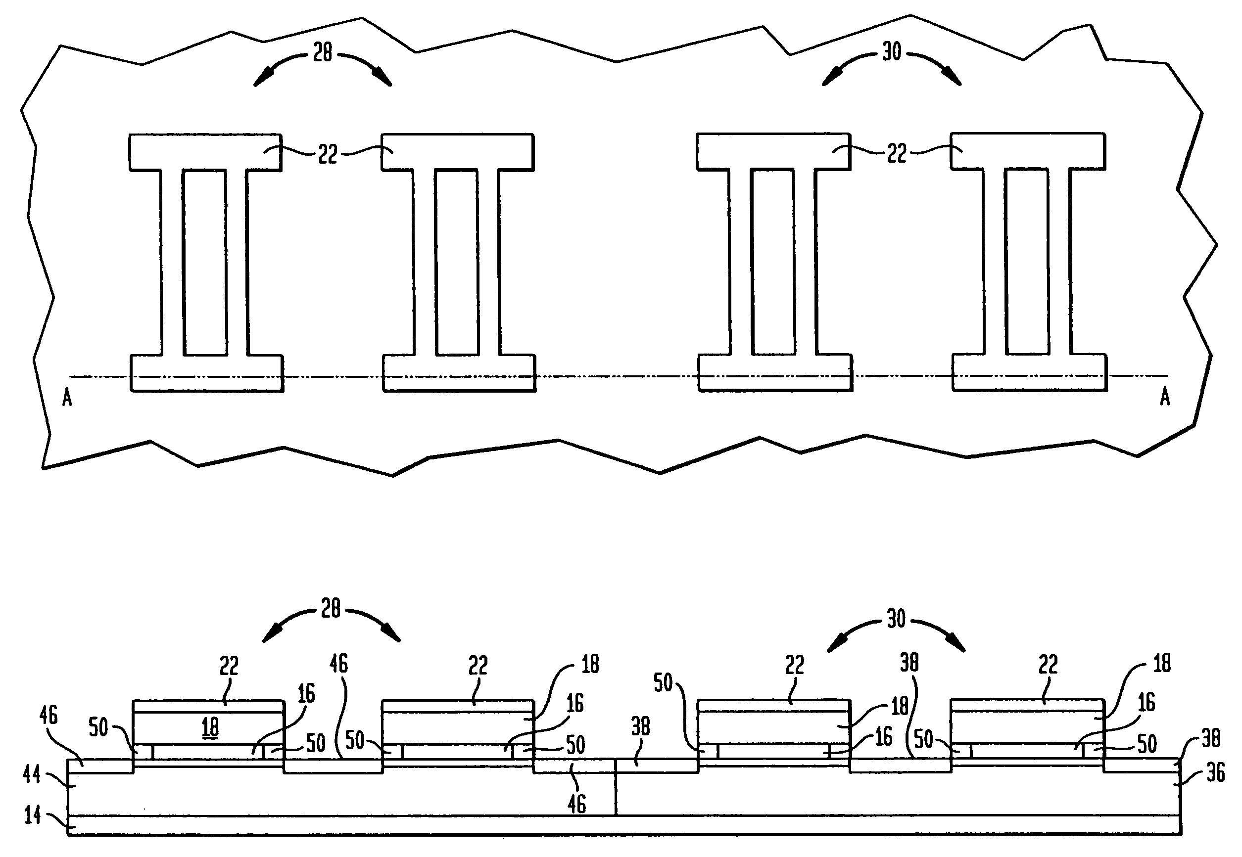
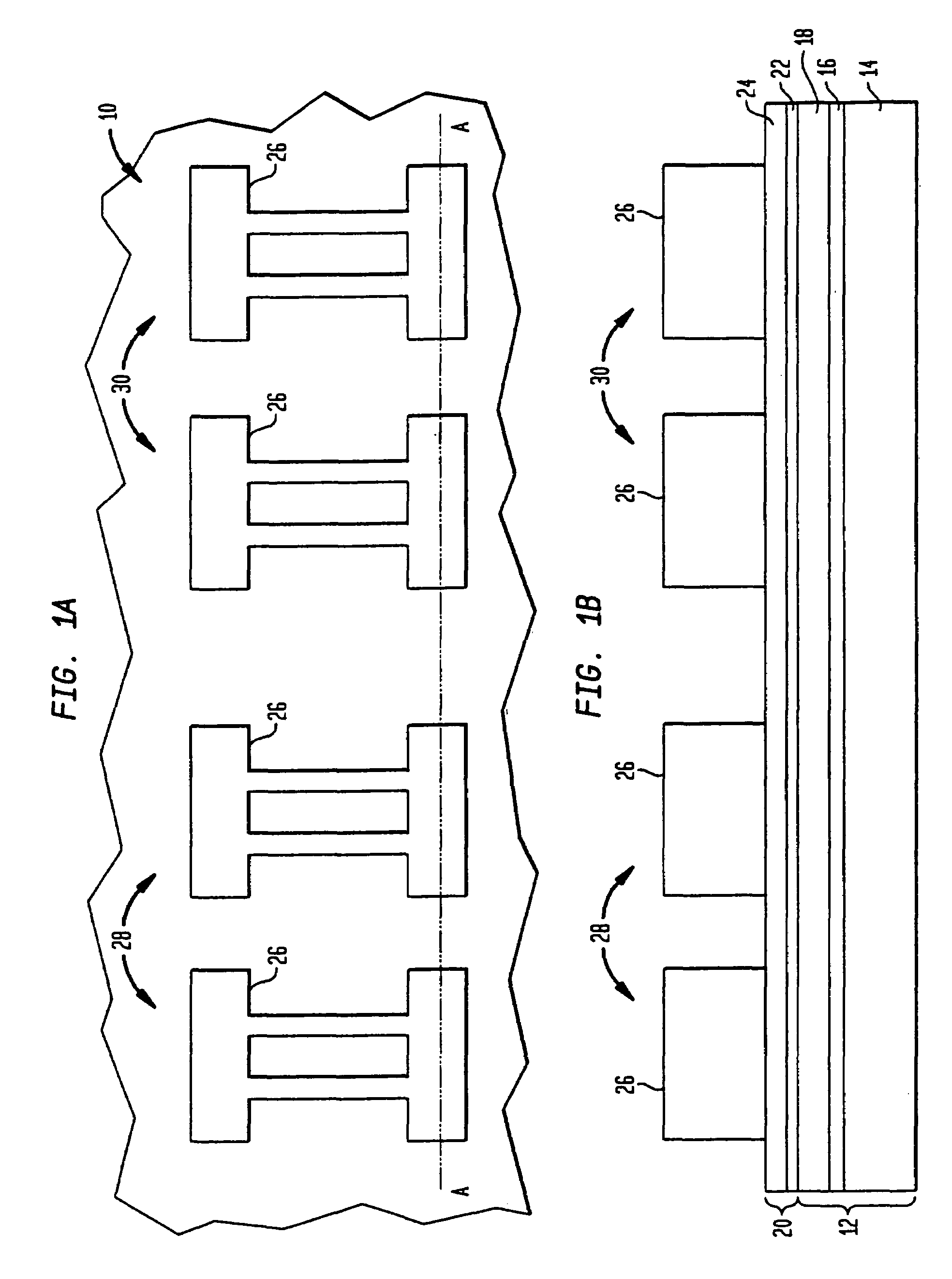
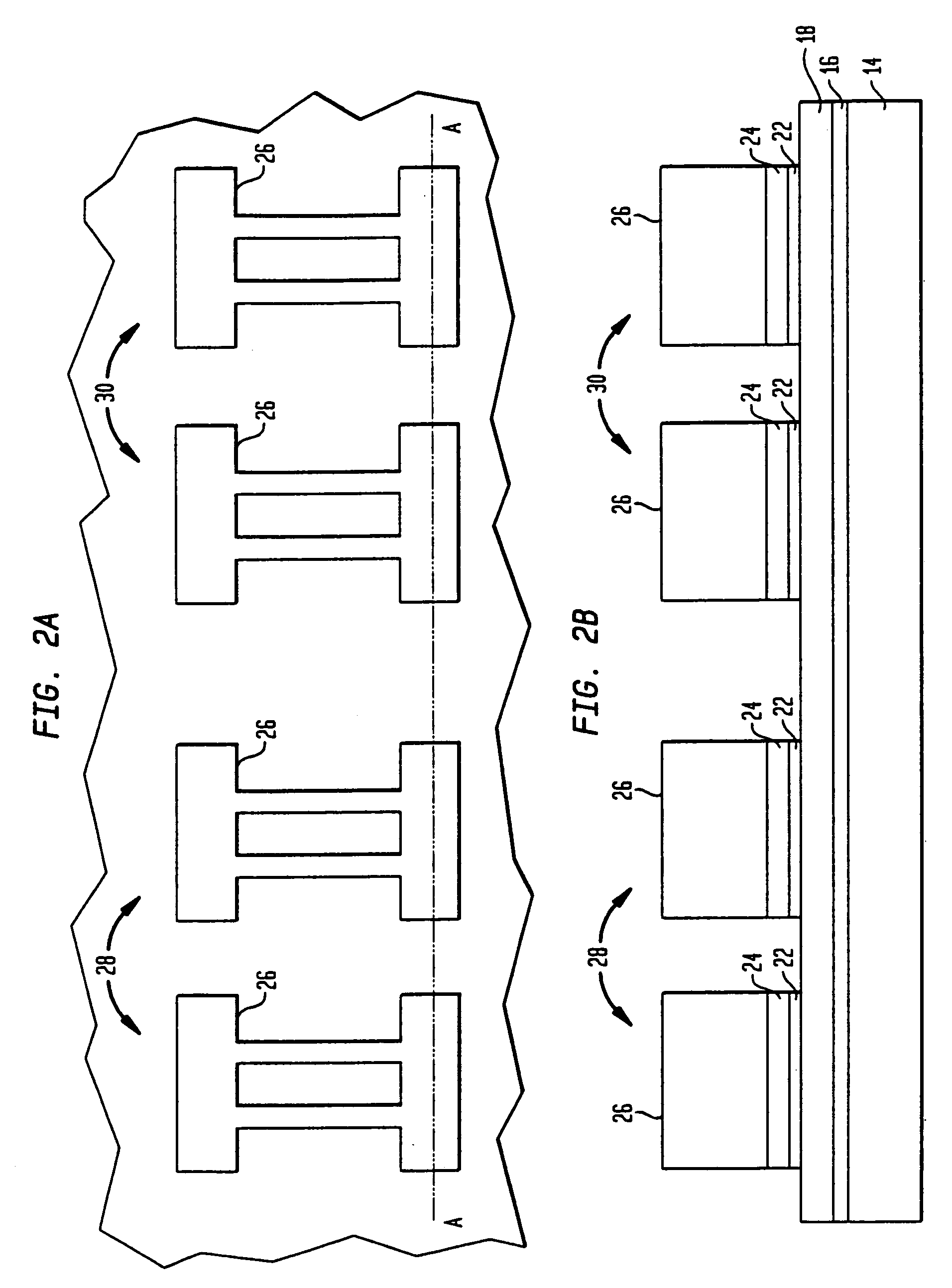
[0040]The present invention, which provides a semiconductor structure including a FinFET in which low capacitance junction-isolation is provided, will now be described in greater detail by referring to the drawings that accompany the present application. It is noted that the drawings of the present application are provided for illustrative purposes and thus they are not drawn to scale. Moreover, the present invention is not limited to a specific number of, or conductivity type, FinFET that can be formed on a bulk semiconductor substrate. For example, it is possible to form an nFinFET or a plurality of nFinFETs, a pFinFET or a plurality of pFinFETs, an nFinFET and a pFinFET or a plurality of nFinFETs and pFinFETs on the same substrate using the method of the present invention. It is noted that in the drawings, a plurality of nFinFETs and a plurality of pFinFETs are shown.

[0041]Each of the drawings of the present invention includes a top down view shown in drawing “A” and a cross-sect...


PUM


Abstract

The present invention provides a SiGe-based bulk integration scheme for generating FinFET devices on a bulk Si substrate in which a simple etch, mask, ion implant set of sequences have been added to accomplish good junction isolation while maintaining the low capacitance benefits of FinFETs. The method of the present invention includes providing a structure including a bottom Si layer and a patterned stack comprising a SiGe layer and a top Si layer on the bottom Si layer; forming a well region and isolation regions via implantation within the bottom Si layer; forming an undercut region beneath the top Si layer by etching back the SiGe layer; and filling the undercut with a dielectric to provide device isolation, wherein the dielectric has an outer vertical edge that is aligned to an outer vertical edge of the top Si layer.

Description

FIELD OF THE INVENTION[0001]The present invention relates to a semiconductor device and a method of fabricating the same. More particularly, the present invention relates to a semiconductor structure including a FinFET in which low capacitance junction-isolation is provided as well as a method of fabricating the semiconductor structure including the FinFET.BACKGROUND OF THE INVENTION[0002]The dimensions of semiconductor field effect transistors (FETs) have been steadily shrinking over the last thirty 30 years or so, as scaling to smaller dimensions leads to continuing device performance improvements. Planar FET devices have a conducting gate electrode positioned above a semiconducting channel, and electrically isolated from the channel by a thin layer of gate oxide. Current through the channel is controlled by applying voltage to the conducting gate.[0003]For a given device length, the amount of current drive for an FET is defined by the device width (w). Current drive scales propor...

Claims


Application Information

Patent Timeline
IPC IPC(8): H01L21/336H01L29/38
CPCH01L21/823431H01L21/823437H01L29/7851H01L29/66795H01L21/823481
Inventor ANDERSON, BRENT A.NOWAK, EDWARD J.
Owner GLOBALFOUNDRIES US INC
Why Eureka
Try Eureka