Method for forming silazane-based dielectric film

a dielectric film and silazane technology, applied in the field of silazane-containing dielectric films, can solve the problems of insufficient filling performance, significant shrinkage of films, and film breakag

Active Publication Date: 2009-06-04
ASM JAPAN
View PDF2 Cites 388 Cited by
  • Summary
  • Abstract
  • Description
  • Claims
  • Application Information

AI Technical Summary

Problems solved by technology

As a result, the film shrinks significantly.
However, the embedded film formed on the thin nitride film shrinks during heat treatment, and this shrinkage generates stress in the silicon nitride film and causes the film to break.
However, reducing the amount of solvent affects the flowability, which leads to insufficient filling performance.
Controlling the thickness of embedded film is difficult because of the material of the foundation film, and this make...

Method used

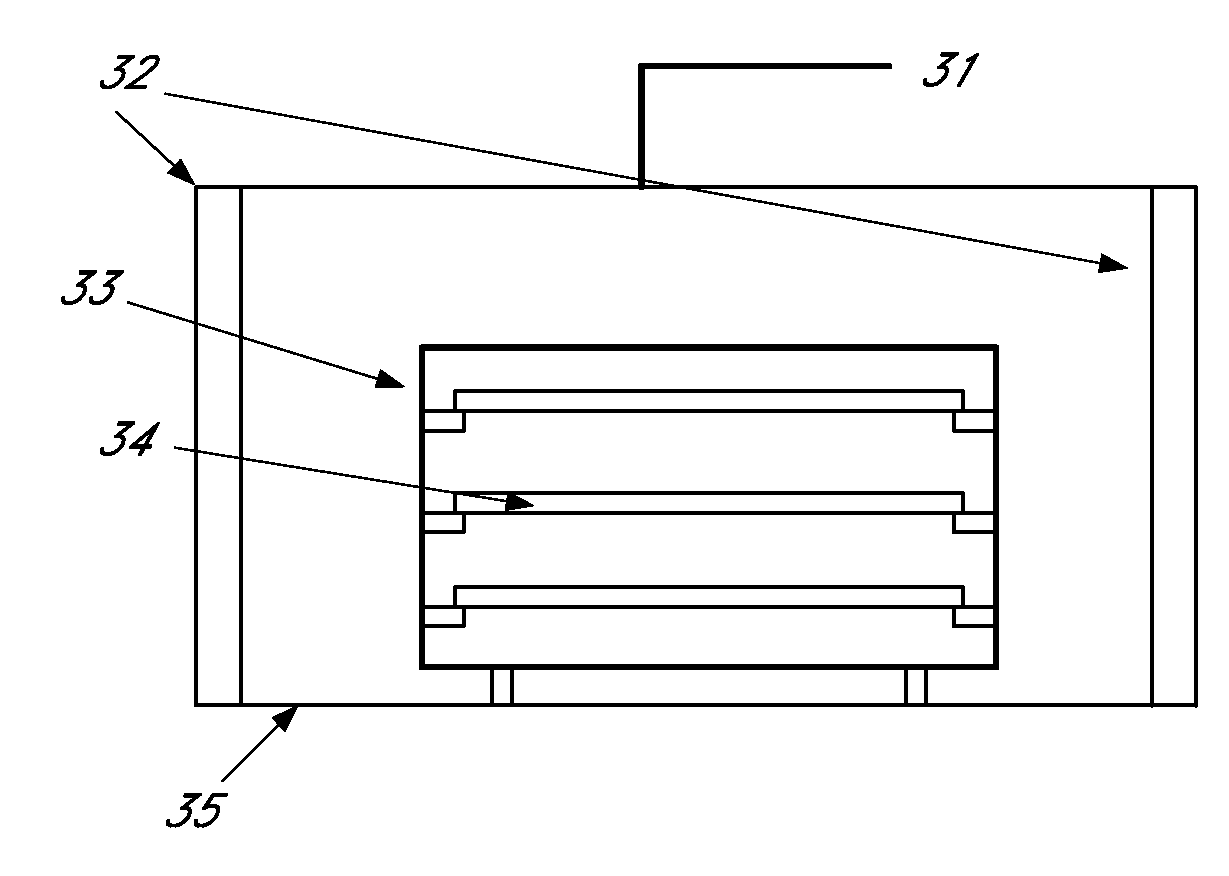
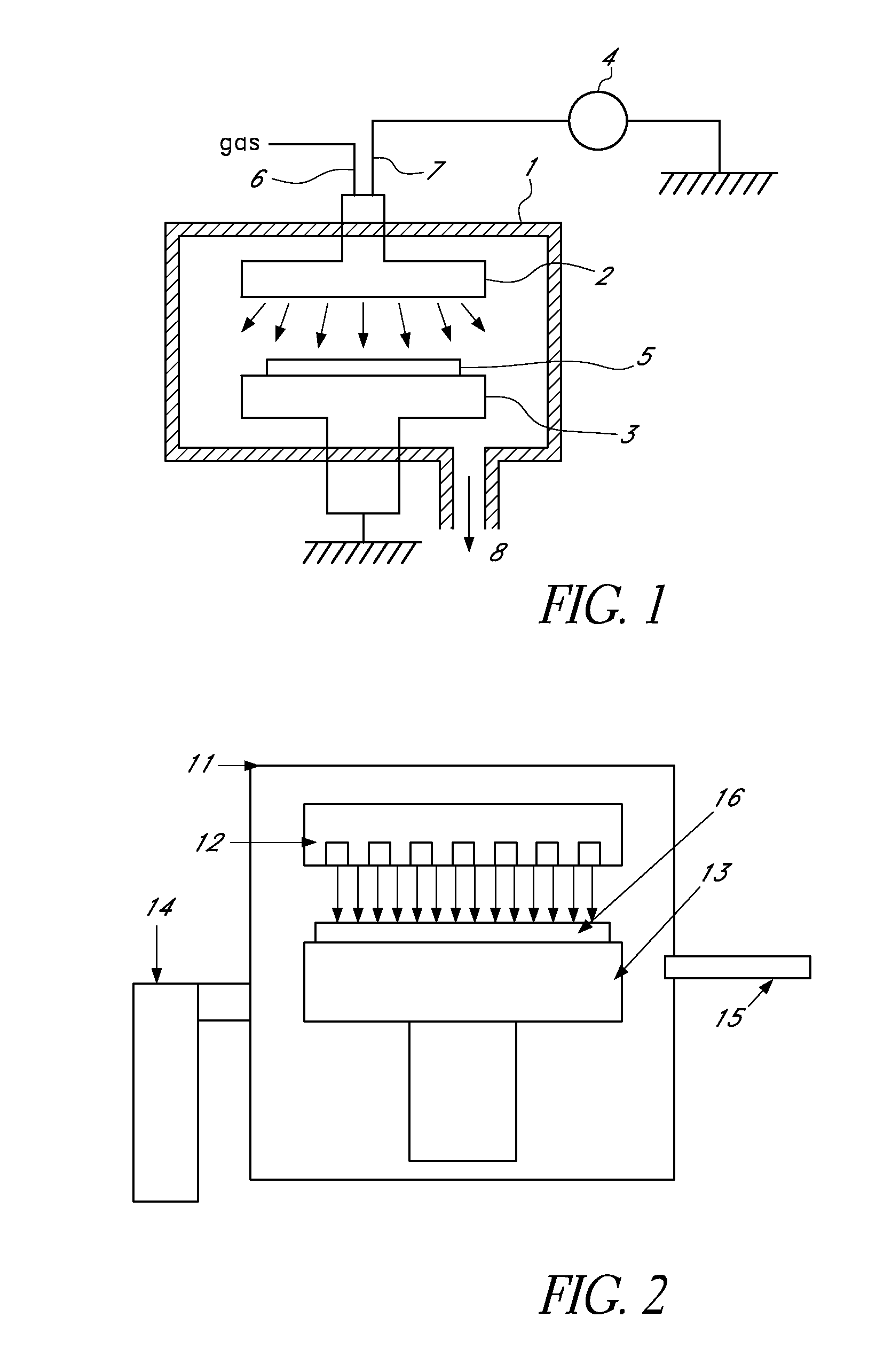
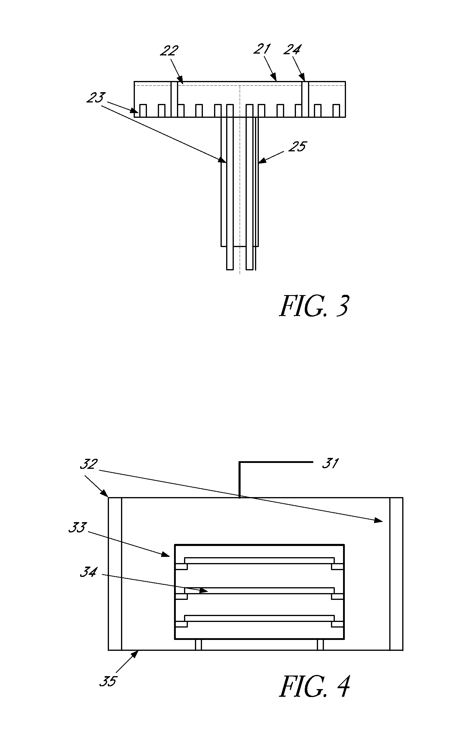

Image

  • Method for forming silazane-based dielectric film
  • Method for forming silazane-based dielectric film
  • Method for forming silazane-based dielectric film

Examples


example 1

Evaluation Results of SiNCH Silazane Process

[0076]Films were formed under the conditions shown in Table 1 and below, and the film characteristics were examined an hour after the heat treatment at 900° C.

[0077]Process Sequence:

[0078]Film forming: Temperature 0° C., pressure 266.6 Pa

[0079]H2O annealing: 1 hour of steam processing at 130° C. (H2O flow rate 1 g / min)

[0080]Heat treatment: 1 hour of O2 / N2 processing at 400° C. (N2 1 SLM, pressure 800 Pa; the experiment was conducted using a chamber separate from the one used for H2O processing.)

[0081]High-temperature heat treatment: 1 hour of N2 processing at 900° C. (N2 flow rate 1 SLM, atmospheric pressure)

[0082]As shown in Table 1, silazane-based films formed without using organic solvent, but using a material containing carbon and an additive gas not containing carbon, exhibited improved filling characteristics through lowering of the RF power when the electrode gap was narrow. When the electrode gap was wide, no problem occurred even ...

example 2

Evaluation Results of SiNH Silazane Process

[0083]Films were formed under the conditions shown in Table 2 and below, and the film characteristics were examined an hour after the heat treatment at 900° C.

[0084]Process Sequence:

[0085]Film forming: Temperature 0° C., pressure 266.6 Pa

[0086]H2O annealing: 1 hour of steam processing at 130° C. (H2O flow rate 1 g / min)

[0087]Heat treatment: 1 hour of O2 / N2 processing at 400° C. (N2 1 SLM, pressure 800 Pa; the experiment was conducted using a chamber separate from the one used for H2O processing.)

[0088]High-temperature heat treatment: 1 hour of N2 processing at 900° C. (N2 flow rate 1 SLM, atmospheric pressure)

[0089]Chemical-solution resistance evaluation: A stock solution of LAL500 was used to conduct the evaluation. A thermal oxide film was used as a reference. The etch rate of the thermal oxide film was 43 nm / min. The decrease in film thickness at the top of the STI structure was calculated based on the cross-section observation result.

[00...

example 3

Dependence of Film Characteristics by Heat Treatment Sequence

[0091]Films were formed under the conditions shown in Table 3 and below, and the film characteristics were examined. The initial surface hardening sequence represents a sequence without H2O annealing, while the initial liquid processing sequence represents one with H2O annealing.

[0092]Film Forming Conditions:

[0093]Susceptor temperature: 0° C.

[0094]Material flow rate: 1,1,3,3-TMDS 30 sccm

[0095]Additive gas flow rate: NH3 20 sccm

[0096]He flow rate: 2 SLM

[0097]Pressure: 266 Pa

[0098]13.56-MHz power: 28 W

[0099]Discharge gap: 400 mm

[0100]The normal logic is that as the film shrinkage increases, the film density increases when the volume of film starts to shrink. As shown in Table 3, however, the film density resulting after H2O annealing was higher than when H2O annealing was not performed, despite the very low film shrinkage rate. A possible cause is the difference in the carbon dissociation and the Si—O replacement steps under...


PUM

PropertyMeasurementUnit
Temperatureaaaaaaaaaa

Abstract

A method of forming a dielectric film includes: introducing a source gas essentially constituted by Si, N, H, and optionally C and having at least one bond selected from Si—N, Si—Si, and Si—H into a reaction chamber where a substrate is placed; depositing a silazane-based film essentially constituted by Si, N, H, and optionally C on the substrate by plasma reaction at −50° C. to 50° C., wherein the film is free of exposure of a solvent constituted essentially by C, H, and optionally O; and heat-treating the silazane-based film on the substrate in a heat-treating chamber while introducing an oxygen-supplying source into the heat-treating chamber to release C from the film and increase Si—O bonds in the film.

Description

BACKGROUND OF THE INVENTION[0001]1. Field of the Invention[0002]The present invention relates generally to a semiconductor technique and more particularly to a silicone-containing dielectric film having good filling or padding property for an interconnect structure of a semiconductor substrate.[0003]2. Description of the Related Art[0004]The requirements for semiconductor processing technologies are increasing as the device nodes continue to become smaller, and the requirements for hard masking are also getting higher to improve the processing performance from dry etching. Also, conventional film forming technologies cannot form desired insulation films in STI and Bit lines, etc., and therefore improvements, modifications and new process applications are being examined.[0005]High-density plasma CVD that provides filling characteristics was first applied to 250-nm node devices, after which the technology was applied to wiring and passivation processes of various devices. As the devic...

Claims


Application Information

Patent Timeline
IPC IPC(8): H01L21/31
CPCC23C16/345H01L21/3185C23C16/45512C23C16/56H01L21/02164H01L21/02167H01L21/0217H01L21/02211H01L21/02219H01L21/02274H01L21/02315H01L21/02337H01L21/02348H01L21/3125C23C16/36
Inventor FUKUZAWA, ATSUKIHA, JEONGSEOKMATSUKI, NOBUO
Owner ASM JAPAN
Why Eureka
Try Eureka