

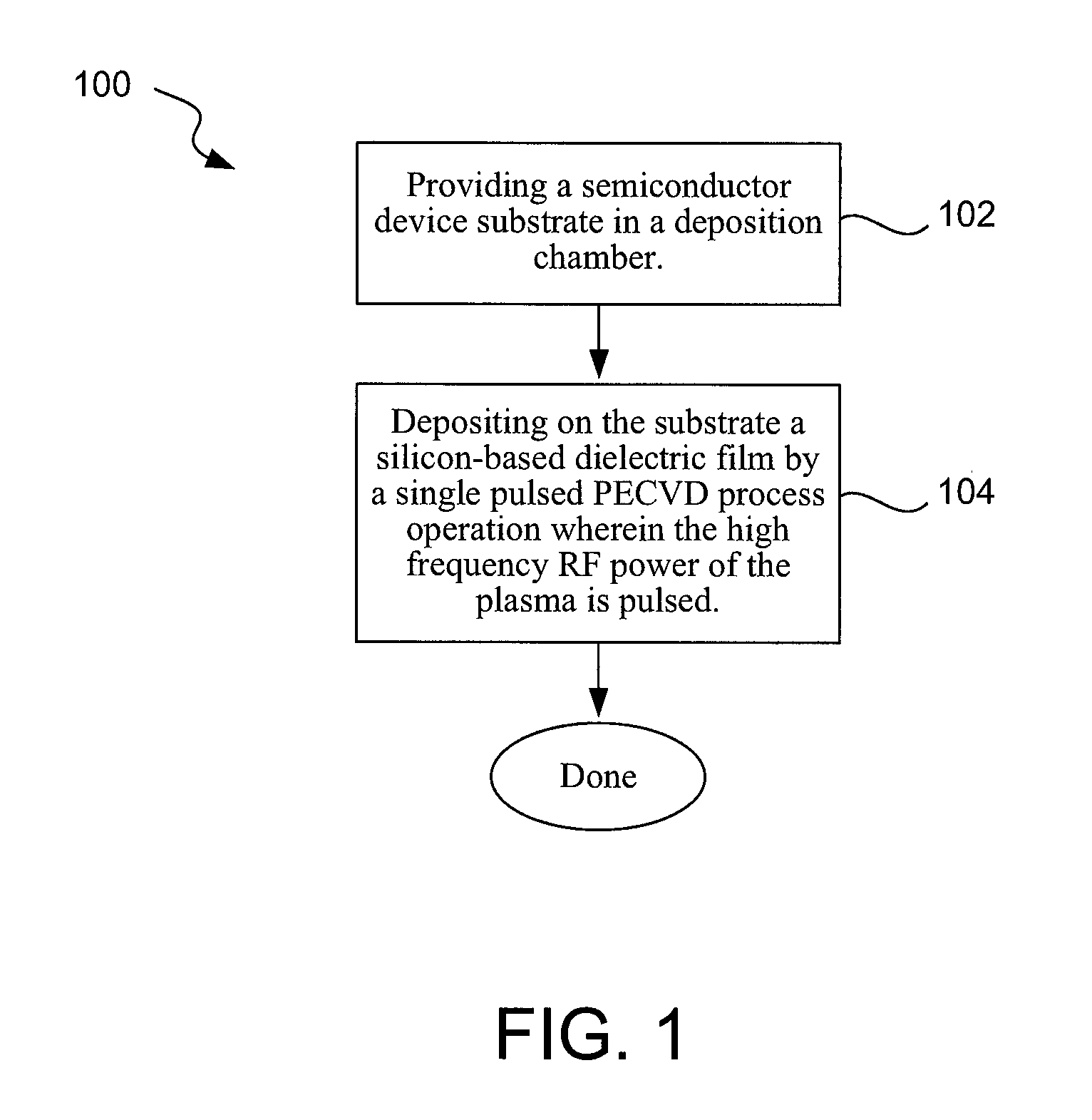
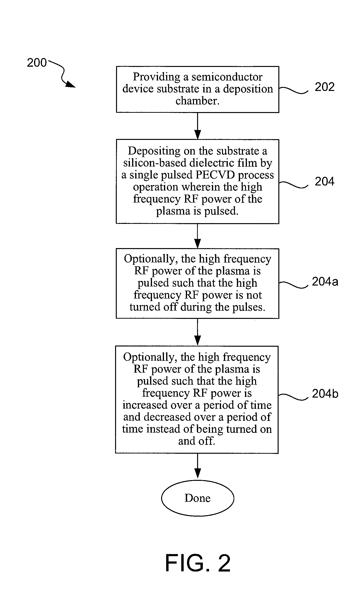
Method for improving process control and film conformality of PECVD film
a technology of pecvd film and process control, applied in the direction of liquid surface applicators, chemical vapor deposition coatings, coatings, etc., can solve the problems of poor conformality, difficult to achieve, and difficult to achieve, so as to improve conformality (or step coverage) and improve the effect of chemical vapor deposition
- Summary
- Abstract
- Description
- Claims
- Application Information
AI Technical Summary
Benefits of technology
Problems solved by technology
Method used
Image

Examples
examples
[0047]The following examples are provided to further illustrate aspects and advantages of the present invention. These examples are provided to exemplify and more clearly illustrate aspects of the present invention and are in no way intended to be limiting.
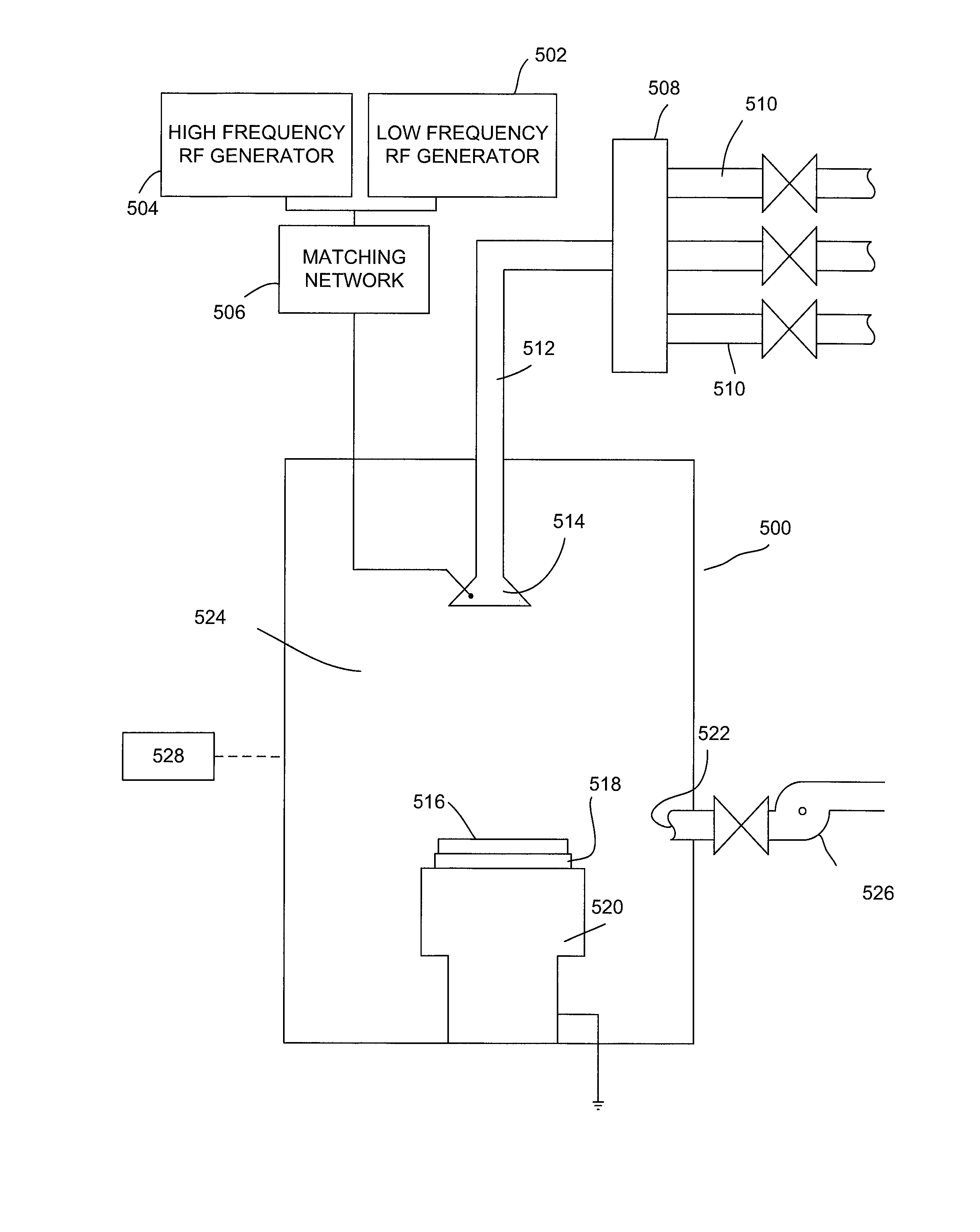
[0048]Film depositions for these examples were conducted in Novellus Vector™ tool with a HFRF source operating at a frequency of 13.56 MHz and with a reactor pressure of about 2 Torr for the oxide deposition and about 9 Torr for the nitride deposition.
[0049]Referring to FIG. 6, the effect of varying the duty cycle in the pulsed plasma enhanced chemical vapor deposition (PECVD) process is illustrated. FIGS. 6a and 6b are plots of the deposited film thickness per unit time the high frequency RF power of the plasma is on (referred to as “thickness per deposition time”) versus duty cycle. FIG. 6a illustrates the effect for a silicon nitride deposition, and FIG. 6b illustrates the effect for a silicon oxide deposition. For silicon nitr...
PUM
| Property | Measurement | Unit |
|---|---|---|
| frequency | aaaaa | aaaaa |
| frequency | aaaaa | aaaaa |
| frequency | aaaaa | aaaaa |
Abstract
Description
Claims
Application Information