Dielectric film and formation method thereof, semiconductor device, non-volatile semiconductor memory device, and fabrication method for a semiconductor device

a semiconductor and non-volatile technology, applied in semiconductor devices, semiconductor/solid-state device details, inorganic insulators, etc., can solve the problems of deterioration of leakage characteristics, difficult to realize a high-performance miniaturized transistor that requires a decrease of the thickness of the gate insulation film, and difficulty in reducing the thickness of the silicon oxide film thus formed. , to achieve the effect of reducing the operational voltage, reducing the leakage current, and increasing the wiring speed

Inactive Publication Date: 2008-11-13
FOUND FOR ADVANCEMENT OF INT SCI
View PDF3 Cites 385 Cited by
  • Summary
  • Abstract
  • Description
  • Claims
  • Application Information

AI Technical Summary

Benefits of technology

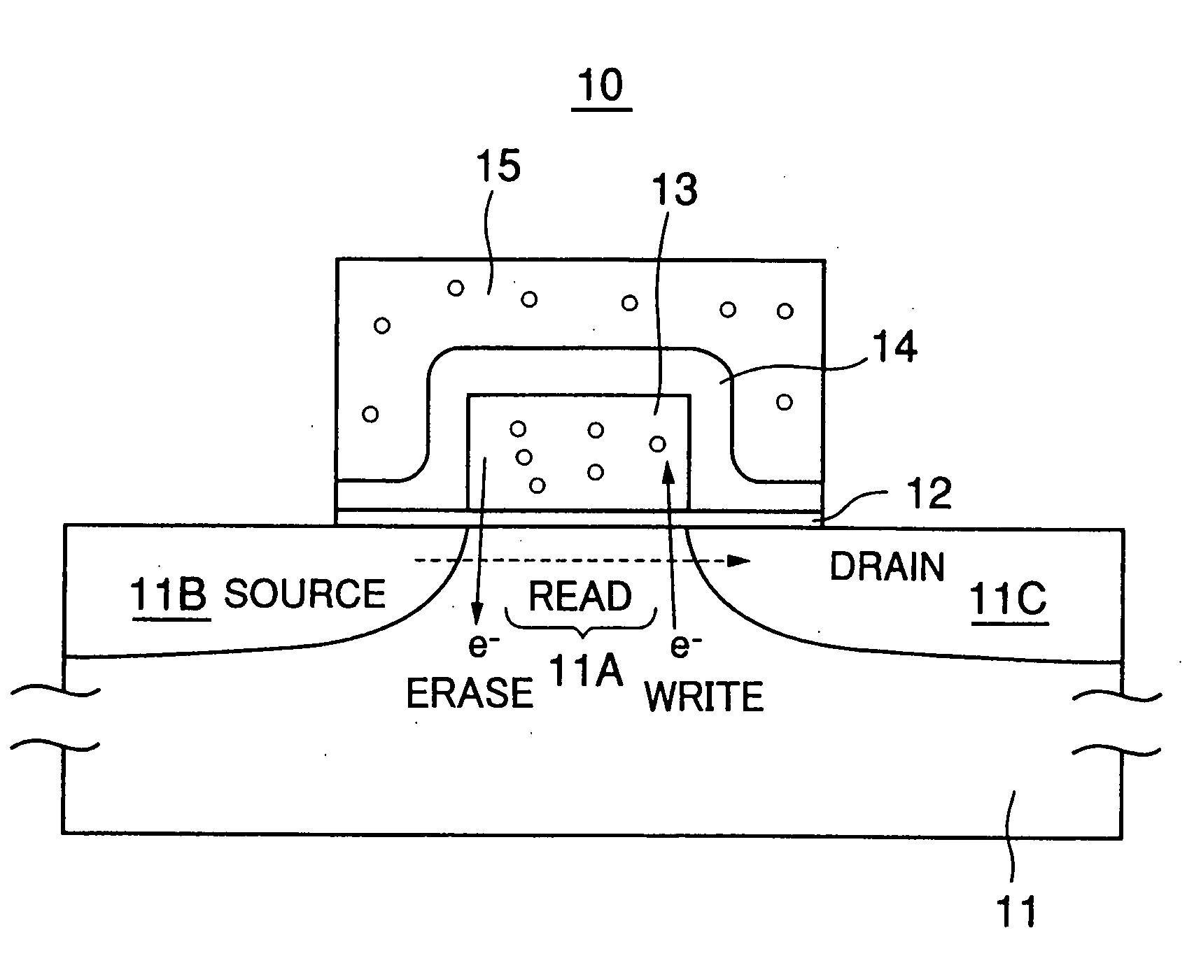
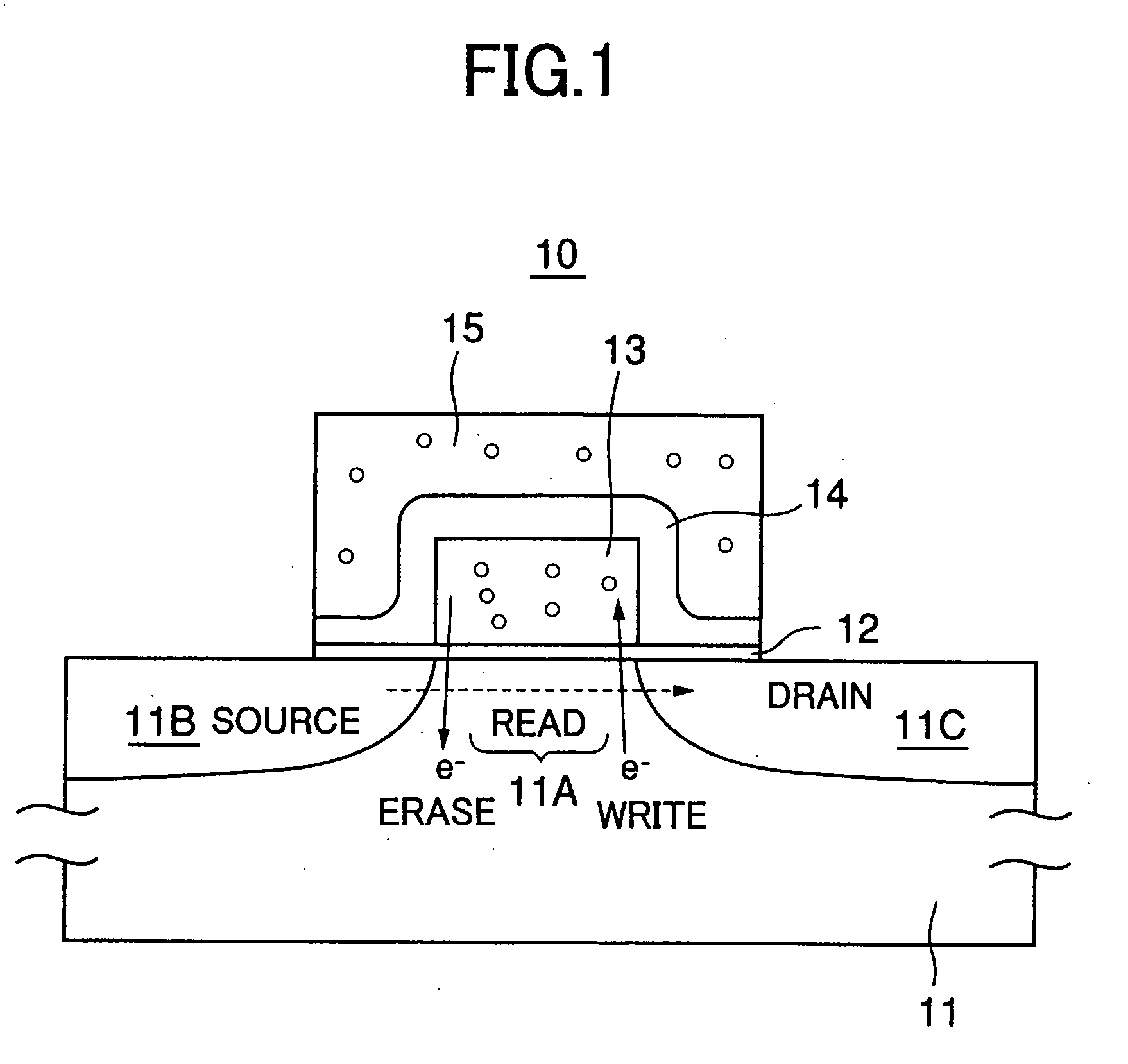
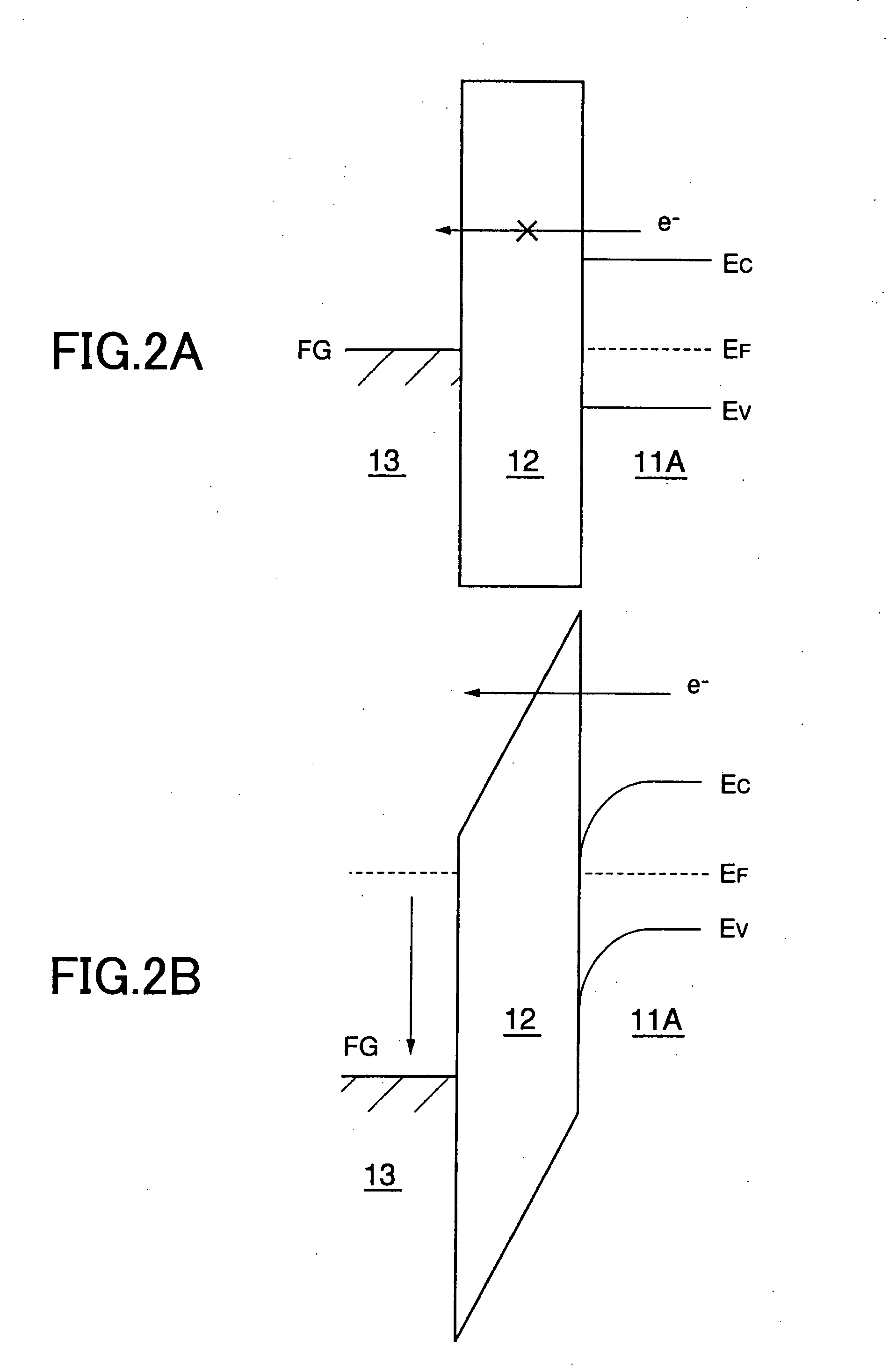
[0062]As a result of using such a dielectric film structure for the tunneling insulation film of the non-volatile semiconductor memory device such as a flash memory, and the like, it becomes possible to increase the wiring speed or reduce the operational voltage while simultaneously reducing the leakage current.
[0063]It should be noted that such an oxide film, in which there is caused nitrogen concentration at the surface part thereof, can be formed also by exposing the silicon surface to microwave plasma formed in a mixed gas of an inert gas primarily formed of Kr, a gas containing nitrogen as a constituent element and a gas containing oxygen as a constituent element. The oxide film thus formed has the composition of an oxynitride film as a whole, while it should be noted that a part of the nitrogen is concentrated in such a structure to the interface between the oxynitride film and the silicon surface for relaxing the stress, while other nitrogen is concentrated to the film surface and forms the desired nitride layer region. In the oxynitride film of such a structure, there is caused stress relaxation by the nitrogen concentrated to the interface to the silicon substrate, and because of this, the density of the electric charges trapped in the film or the density of the interface state is reduced and the leakage current path other than the tunneling mechanism is effectively blocked. Thus, the oxynitride film obtained according to such a process has an extremely high film quality. In such an oxynitride film, it is preferable that the hydrogen concentration contained in the film is 1012 cm−2 or less, preferably 1011 cm−2 or less in terms of surface density.
[0064]As the formation of the dielectric film can be conducted at a low temperature of 550° C. or less in the present invention, it is possible to recover the oxygen defects in the film without decoupling the hydrogen terminating the dangling bonds in the oxide film. This applies also to the formation of the nitride film or oxynitride film to be explained later.

Problems solved by technology

Further, it is known that there arises a remarkable deterioration of leakage characteristics when the thickness of the silicon oxide film thus formed by the conventional thermal oxidation process is reduced to about 2 nm or less.
Thus, it has been difficult to realize a high-performance miniaturized transistor that requires decrease of the gate insulation film thickness.
Further, when the silicon oxide film is formed on a silicon crystal having a surface orientation other than the orientation or on a polysilicon formed on an insulation film, there arises a problem of formation of large interface state density at the oxide / silicon interface as compared with when the silicon oxide film is formed on the -oriented silicon surface, and this holds true even when the silicon oxide film is formed by thermal oxidation.
Thus, such a silicon oxide film has poor electric properties in terms of breakdown characteristics, leakage current characteristics, and the like, particularly when the thickness thereof is reduced, and there has been a need of increasing the film thickness of the silicon oxide film when using such a silicon oxide film.
In the conventional thermal oxidation process, it should be noted that there has been a large fluctuation of oxidation reaction rate caused by temperature fluctuation, and it has been difficult to conduct the production process of semiconductor devices with high throughput while using a large-area substrate.
Particularly, it has not been possible to obtain the desired low leakage current characteristics in the case the silicon oxide film has a thickness of about 2 nm or less on the silicon substrate surface.
Thus, it has been difficult to realize high-performance, miniaturized transistors that require a further decrease of the gate insulation film thickness, similarly to the case of conventional thermal oxide film formation technology.
Further, there has been a problem that the silicon oxide film thus formed shows severe degradation of electric properties in the case the silicon oxide film is used for a transistor, such as degradation of conductance caused by hot carrier injection or increase of leakage current in the case the silicon oxide film is used in a device such as a flash memory, which relies upon tunneling of electrons caused through the silicon oxide film, as compared with the case of using a silicon oxide film formed by the conventional thermal processes.

Method used


Image

  • Dielectric film and formation method thereof, semiconductor device, non-volatile semiconductor memory device, and fabrication method for a semiconductor device
  • Dielectric film and formation method thereof, semiconductor device, non-volatile semiconductor memory device, and fabrication method for a semiconductor device
  • Dielectric film and formation method thereof, semiconductor device, non-volatile semiconductor memory device, and fabrication method for a semiconductor device

Examples


first embodiment

[0097]FIGS. 4A-4C show the low-temperature formation process of an oxide film that uses plasma as well as the fabrication process of a semiconductor device that uses such an oxide film according to a first embodiment of the present invention. Further, FIG. 5 shows an example of a plasma processing apparatus used in the present invention and having a radial line slot antenna in a cross-sectional view.

[0098]In the present embodiment, the hydrogen terminating the dangling bonds at a silicon surface is first removed in the step of FIG. 4A. More specifically, the removal process of the surface-terminating hydrogen and the oxidation process are conducted in the same processing chamber continuously, and the Kr gas, which is used for the plasma excitation gas in the subsequent oxide film formation process, is used in the removal process of the surface-terminating hydrogen.

[0099]First, a vacuum vessel (processing chamber) 101 is evacuated in the plasma processing apparatus of FIG. 5 and an A...

second embodiment

[0127]FIGS. 11A-11C show the formation method of a nitride film at low temperature by using plasma according to a second embodiment of the present invention, as well as the fabrication method of a semiconductor device that uses such a nitride film.

[0128]In the present embodiment, too, an apparatus similar to the one shown in FIG. 5 is used for the nitride film formation. Further, in the present embodiment, it is preferable to use Ar or Kr for the plasma excitation gas for removing the terminating hydrogen and for the nitride film formation, in order to form a high-quality nitride film.

[0129]Hereinafter, an example of using Ar will be represented.

[0130]First, the interior of the vacuum vessel (processing chamber) 101 of FIG. 5 is evacuated to a vacuum state in the step of FIG. 11A and an Ar gas is introduced from the shower plate 102 such that the pressure inside the processing chamber is set to about 13.3 Pa (100 mTorr).

[0131]Next, a silicon substrate 103 is introduced into the proc...

third embodiment

[0148]FIGS. 13A-13D show the formation method of a two-layer laminated dielectric structure according to a third embodiment of the present invention in which an oxide film and nitride film formed by the low-temperature plasma process are laminated, as well as a fabrication process of a semiconductor device that uses such a two-layer laminated dielectric structure.

[0149]It should be noted that the apparatus used for the formation of the oxide film and the nitride film in the present embodiment is identical with the apparatus of FIG. 5. In the present embodiment, Kr is used for the plasma excitation gas at the time of formation of the oxide film and the nitride film.

[0150]First, in the step of FIG. 13A, the vacuum vessel (processing chamber) 101 is evacuated to the vacuum state and an Ar gas is introduced into the processing chamber 101 from the shower plate 102. Next, the gas to be introduced next is switched to the Kr gas from the initial Ar gas, and the pressure of the processing c...


PUM

PropertyMeasurementUnit
temperatureaaaaaaaaaa
thicknessaaaaaaaaaa
electric fieldaaaaaaaaaa

Abstract

In a film formation method of a semiconductor device including a plurality of silicon-based transistors or capacitors, there exist hydrogen at least in a part of the silicon surface in advance, and the film formation method removes the hydrogen by exposing the silicon surface to a first inert gas plasma. Thereafter a silicon compound layer is formed on the surface of the silicon gas by generating plasma while using a mixed gas of a second inert gas and one or more gaseous molecules, such that there is formed a silicon compound layer containing at least a pat of the elements constituting the gaseous molecules, on the surface of the silicon gas.

Description

CROSS-REFERENCE TO RELATED APPLICATIONS[0001]This application is a divisional of U.S. patent application Ser. No. 10 / 451,925 filed Jun. 27, 2003 which is a national phase of PCT / JP01 / 11596 filed Dec. 27, 2001, which claims priority to Japanese patent application Serial no. 2000-402834 filed Dec. 28, 2000 and Japanese patent application Serial no. 2001-094246 filed Mar. 28, 2001.BACKGROUND OF THE INVENTION[0002]The present invention relates to a semiconductor device in which an oxide film, a nitride film, an oxynitride film, and the like, is formed on a silicon semiconductor, and the formation method thereof.[0003]The gate insulation film of a MIS (metal / insulator / silicon) transistor is required to have various high-performance electric properties and also high reliability, such as low leakage current characteristic, low interface state density, high breakdown voltage, high resistance against hot carriers, uniform threshold voltage characteristic, and the like.[0004]In order to satis...

Claims


Application Information

Patent Timeline
Patent Type & Authority Applications(United States)
IPC IPC(8): H01L29/788H01L23/58H01L21/469H01L21/3205H01B3/00H01B3/02H01L21/28H01L21/306H01L21/314H01L21/316H01L21/318H01L21/336H01L21/8234H01L21/8239H01L21/8246H01L21/8247H01L27/105H01L27/115H01L27/12H01L29/49H01L29/51H01L29/786H01L29/792
CPCH01L21/0214H01L21/02164H01L21/0217H01L21/02238H01L21/02247H01L21/02249H01L21/02252H01L21/02315H01L21/02332H01L21/0234H01L21/28202H01L21/28211H01L21/2822H01L21/30604H01L21/3144H01L21/31662H01L21/3185H01L21/823462H01L27/105H01L27/11526H01L27/11546H01L27/11568H01L27/12H01L29/4908H01L29/513H01L29/517H01L29/518H01L29/66757H01L29/78603H01L29/78645H01L27/1052H10B99/00H10B41/40H10B41/49H10B43/30H01L21/18
Inventor OHMISUGAWA, SHIGETOSHIHIRAYAMA, MASAKISHIRAI, YASUYUKI
Owner FOUND FOR ADVANCEMENT OF INT SCI
Why Eureka
Try Eureka