Three-Dimensional Adhesive Device Having a Microelectronic System Embedded Therein

a three-dimensional adhesive and microelectronic system technology, applied in the field of micro electronic systems, can solve the problems of occluding adhesives, inconvenient use, and inability to disclose constructs, and achieve the effects of reducing the number of microelectronic systems, and improving the accuracy of the application

Inactive Publication Date: 2008-11-06
BRAEMAR MFG +2
View PDF55 Cites 385 Cited by
  • Summary
  • Abstract
  • Description
  • Claims
  • Application Information

AI Technical Summary

Benefits of technology

[0299]One special advantage of the invention is the simple and inexpensive way of preparing an adhesive body having a three-dimensional shape from a pressure sensitive adhesive.
[0300]As mentioned above, the pressure sensitive adhesives are either a thermoplastic pressure sensitive adhesive or it is a chemically curable adhesive that has the ability to be moulded into a three-dimensional shape.
[0301]The thermoplastic pressure sensitive adhesive may typically enter a fluid condition and achieve a moderate viscosity at above 100-120 deg C. i.e. above the glass transition temperature of the composition, which makes it easy to mould the adhesive composition to the desired shape. One example may be direct moulding. In a first step the cover layer is provided in the desired shape at temperatures just below the glass transition temperature of the cover film and then the necessary amount of adhesive is filled the into the mould to fill up the mould. The filling of the mould may be in two steps whenever appropriate. This will allow partly filling with the molten adhesive in a second step, placing the electronic parts in a third step and eventually filling and covering the electronic parts with the remainder of the adhesive in a fourth step. As a last step a release liner is applied and then the adhesive device is punched out of the mould.
[0302]Alternatively the adhesive laminated with the cover film may be processed through compression, pressing or moulding into the desired geometry or shape at elevated temperature, but slightly below the glass transition temperature of the adhesive. Optionally the microelectronic system may be placed between two layers of adhesives and then moulded. The moulding is performed in the press at elevated temperature and if desired with the microelectronic system placed in the mould preferably in the centre of the mould.
[0303]In the special embodiment where exchangeable or reusable components are a part of the adhesive device, a female and a male part of a moulding shape is required.
[0304]In another embodiment of the invention curable pressure sensitive adhesive is cast in the desired shape. The casting may follow the same principles as of above allowing a partial filling step of the mould with the cover film, applying the electronic components and thereafter complete the filling of adhesive in the mould and finally concluding with placing the release liner, curing if necessary and die cutting.

Problems solved by technology

However, the adhesives used are occluding.
For any practical purpose the disclosed constructs will be useless as the moisture from the hydrogel will migrate into the hydrocolloid adhesive and disrupt this over time.
However, in this respect the known microelectronic systems suffer from several major drawbacks as described below.
Attachment to the skin by means of occlusive pressure sensitive adhesives often leads to skin irritation due to the occlusion of moisture and due to irritants, such as monomers from the pressure sensitive adhesive polymer system, e.g. from for instance acrylic adhesives.
Irritation may be the in form of itching and erythema and may especially develop when the adhesive device is attached for a prolonged period of time.
Occlusion may also increase the risk of creating allergy to the adhesive composition.
One often used way to solve the negative effects of occlusion is to use micro porous tapes, but such tapes are essentially two-dimensional and thin and does not protect the microelectronic system from shear forces due to friction against clothes and the like.
In the above references, the devices are attached to the skin by thin planar adhesive layers carrying the microelectronic system as a bulky part leading to discomfort of the patient or person carrying the device due to stiffness or friction against clothing and increasing the risk of involuntarily detachment from the skin.
However, a fairly thick layer may show a tendency of adhering at the edge to clothing or linen and by doing so a tendency to roll and detach is created.
The disadvantage of such a system is that the patient does not have freedom to move since the wires are attached to the sensors on the body and connected to a monitoring system.
Often these medical devices are only attached for a limited period of time until a disease is diagnosed or a patient's health has improved.
The different elements have different lifespan, however, since the elements are typically assembled in one inseparable unit they are all disposed after use.
However, the microelectronic element may be reused a large number of times thereby making it an expensive element to dispose after one use only.

Method used


Image

  • Three-Dimensional Adhesive Device Having a Microelectronic System Embedded Therein
  • Three-Dimensional Adhesive Device Having a Microelectronic System Embedded Therein
  • Three-Dimensional Adhesive Device Having a Microelectronic System Embedded Therein

Examples


example 1

[0323]Three batches of adhesive were produced. The adhesives were prepared by standard hot melt procedure in a Herman Linden z-blade mixer (Machine type LK 110.5), by mixing the components of elastomer (Kraton), one third of the plasticiser (DOA) and the resin (Arkon) at 130 degree C. until a homogeneous mixture was achieved (30-50 minutes). The rest of the plasticiser and the hydrocolloid filler (CMC) was added and the mixture was blended for 20 minutes.

Recipe 1Recipe 2Recipe 3Kraton 116118.019.015.0(Shell)Arkon P9032.036.0(ArakawaDOA5.67.5(Dioctyl adipate)Vistanex ® LM-45.0MH (Exxon)CMC: Blanose44.437.540.09H4XF(Hercules)

example 2

Moulded Bodies of the Adhesives of Example 1

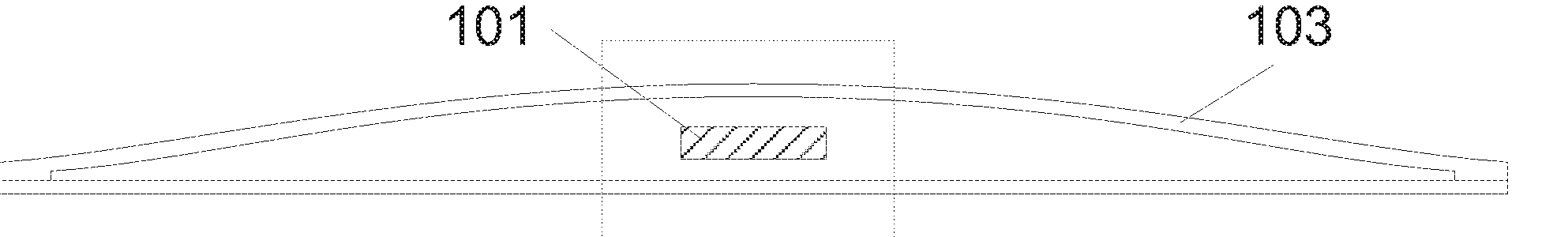
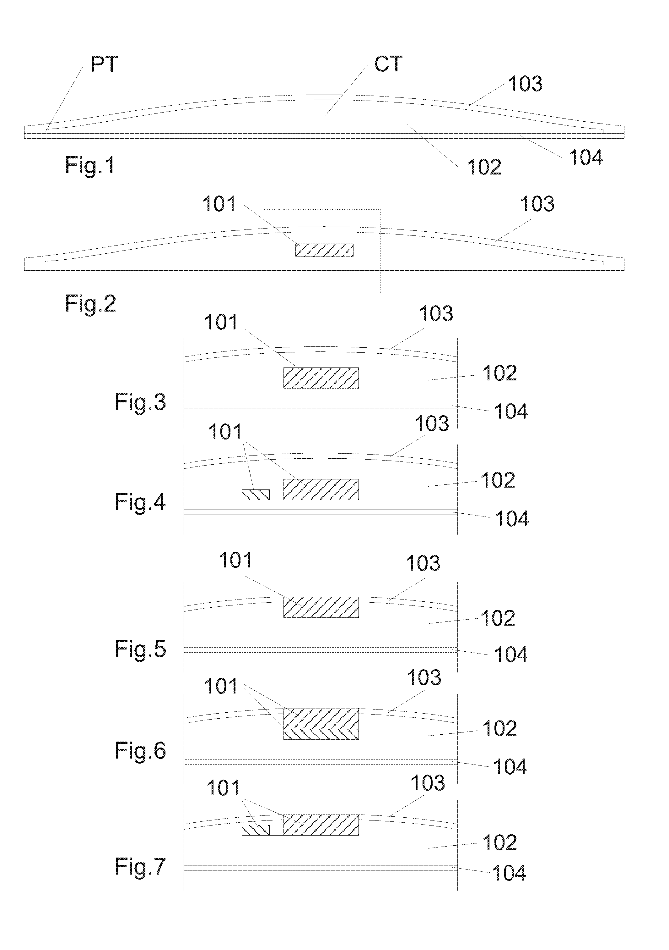
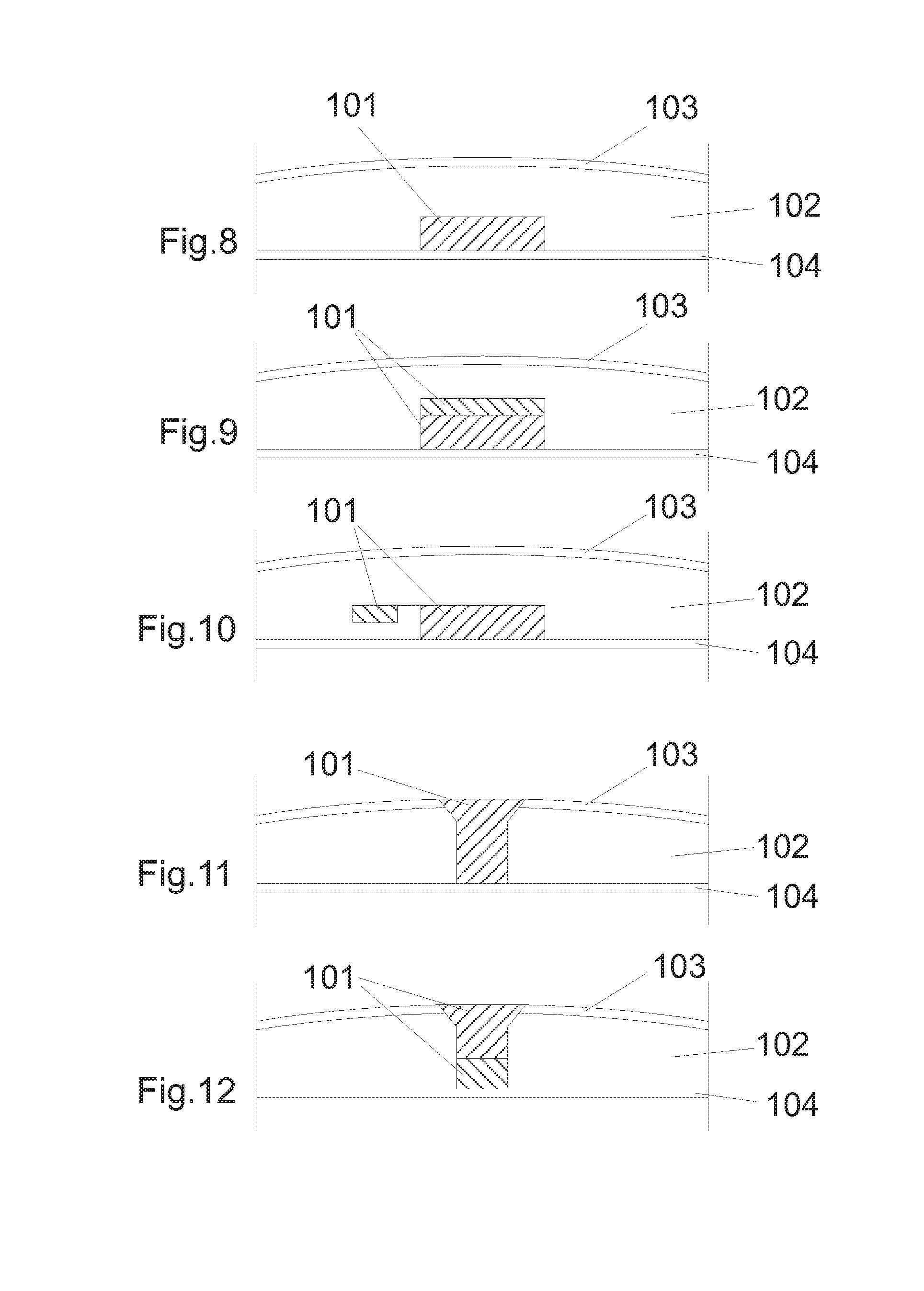
[0324]Each of the adhesives according to claim 1 were applied on to a 35 micrometer thick cover film of polyethylene and a siliconised polyethylene liner was applied to the opposite side of the adhesive patch and pressed to the desired shape according to any of the illustrations 1-3 in a for the shape designed mould at 90 degree C. by altering the non-cavity holding mould to give the shape of the recess. The centre of the adhesive device was 3.4 mm and the thickness of the outer rim 0.4 mm.

example 3

Moulded Silicone Pressure Sensitive Adhesive Body

[0325]Dow Corning 7-9800 A&B (mixing ration between A and B is 1:1 by weight) were used for production of a PDMS based adhesive body. A mould having a triangular shape (each side of the triangular mould having a distance of 300 mm, the center part having a thickness of 0.5 mm and the edge having a thickness of 0.1 mm) was used. The components were thoroughly mixed and applied on a 50 μm cover layer of silicone rubber lining in the female part of a triangular mould and a male mould part was placed on top, said part lined with a low density polyethylene release liner. The adhesive was cured in an oven at 100 degree C. for 15 minutes. After curing the adhesive was punched out of the mould and a dent in the centre of the adhesive body device for embedment of an electronic sensing system was punched out.


PUM

PropertyMeasurementUnit
thicknessaaaaaaaaaa
thicknessaaaaaaaaaa
thicknessaaaaaaaaaa

Abstract

Accordingly, the present invention relates to a three-dimensional adhesive device to be attached to the body surface of a mammal comprising a microelectronic sensing system characterized by(a) a three-dimensional adhesive body made of a pressure sensitive adhesive having an upper surface and a bottom surface;(b) a microelectronic system embedded in the body of the pressure sensitive adhesive;(c) one or more cover layer(s) attached to the upper surface; and(d) optionally a release liner releasable attached to the bottom surface of the adhesive device.Suitably the microelectronic system is a microelectronic sensing system capable of sensing physical input such as pressure, vibration, sound, electrical activity (e.g. from muscle activity), tension, blood-flow, moisture, temperature, enzyme activity, bacteria, pH, blood sugar, conductivity, resistance, capacitance, inductance or other chemical, biochemical, biological, mechanical or electrical properties.

Description

FIELD OF INVENTION[0001]The invention relates to micro electronic systems predominantly for monitoring physiological or neurological conditions. More particular the invention relates to invasive and non-invasive microelectronic systems embedded in a three-dimensional adhesive device, which may be attached to the surface, suitably the skin, of a mammal. The microelectronic systems suitably utilises wireless communication and are useful for measuring ECG (Electro CardioGraphy), EMG (Electro MyoGraphy), EEG (Electro EncephaloGraphy), blood glucose, pulse, blood pressure, pH, and oxygen.BACKGROUND[0002]The attachment of sensing systems to the skin by means of pressure sensitive adhesives is well established. Thus, AMBU A / S, DK has a number of products for measuring ECG, which is attached to the skin by foam adhesives, micro-porous adhesives or hydrogel adhesives. These sensors are in general connected with wires to a monitoring device.[0003]In WO 03 / 065926 A2 Ozgus et al disclose a wear...

Claims


Application Information

Patent Timeline
Patent Type & Authority Applications(United States)
IPC IPC(8): A61B5/04B32B33/00B23P17/00B28B3/02A61B5/296A61B5/308
CPCA61B5/0002Y10T29/49002A61B5/024A61B5/04087A61B5/0478A61B5/0492A61B5/14532A61B5/14539A61B5/14542A61B5/14546A61B5/411A61B5/6833A61B2560/0412A61B2562/08A61B5/6832Y10T428/14A61B5/02A61B5/68335A61B5/259A61B5/291A61B5/296
Inventor FAARBAEK, SUSANNE HOLMHOPPE, KARSTENSAMUELSEN, PETER BOMANBRANEBJERG, JENS
Owner BRAEMAR MFG
Why Eureka
Try Eureka