Conductor pattern structure of capacitive touch panel

a capacitive touch panel and pattern structure technology, applied in the field of capacitive touch panel devices, can solve the problems of complex manufacturing of capacitive touch panels, high thickness of panel structures, and trend of miniaturization, and achieve the effects of reducing structure thickness, simple process, and simplifying structur

Active Publication Date: 2008-10-30
TRENDON TOUCH TECHNOLOGY CORPORATION
View PDF12 Cites 371 Cited by
  • Summary
  • Abstract
  • Description
  • Claims
  • Application Information

AI Technical Summary

Benefits of technology

[0018]According to the present invention, a plurality of first-axis conductor assemblies and a plurality of second-axis conductor assemblies, which constitute the conductor pattern structure of a capacitive touch panel, are formed on the same surface of a substrate, thereby simplifying the structure and reducing the thickness of the structure. When the conductor cells of the first-axis conductor assemblies and the conductor cells of the second-axis conductor assemblies that are adjacent to each other are touched by a user's finger, a capacitance variation signal is induced, in response to the area of the adjacent conductor cells on which the finger of the user is laid, and then applied to a control circuit to identify the position where the user's finger touches the panel. The first-axis conductor assemblies and the second-axis conductor assemblies of the conductor pattern structure can be formed on only one surface of the substrate by the general circuit laying techniques. Thus, the present invention can be practiced in a simple process with high passing rate and low costs.

Problems solved by technology

This makes the structure of the panel very thick and is thus against the trend of miniaturization.
This complicates the manufacturing of the capacitive touch panel.

Method used


Image

  • Conductor pattern structure of capacitive touch panel
  • Conductor pattern structure of capacitive touch panel
  • Conductor pattern structure of capacitive touch panel

Examples


first embodiment

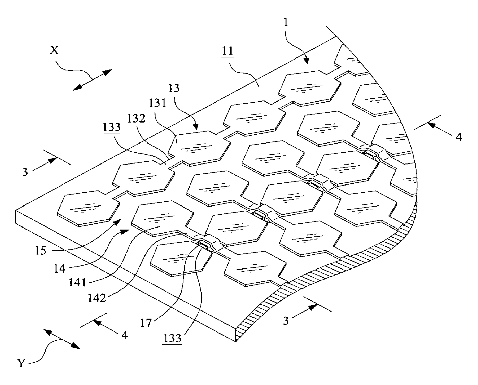
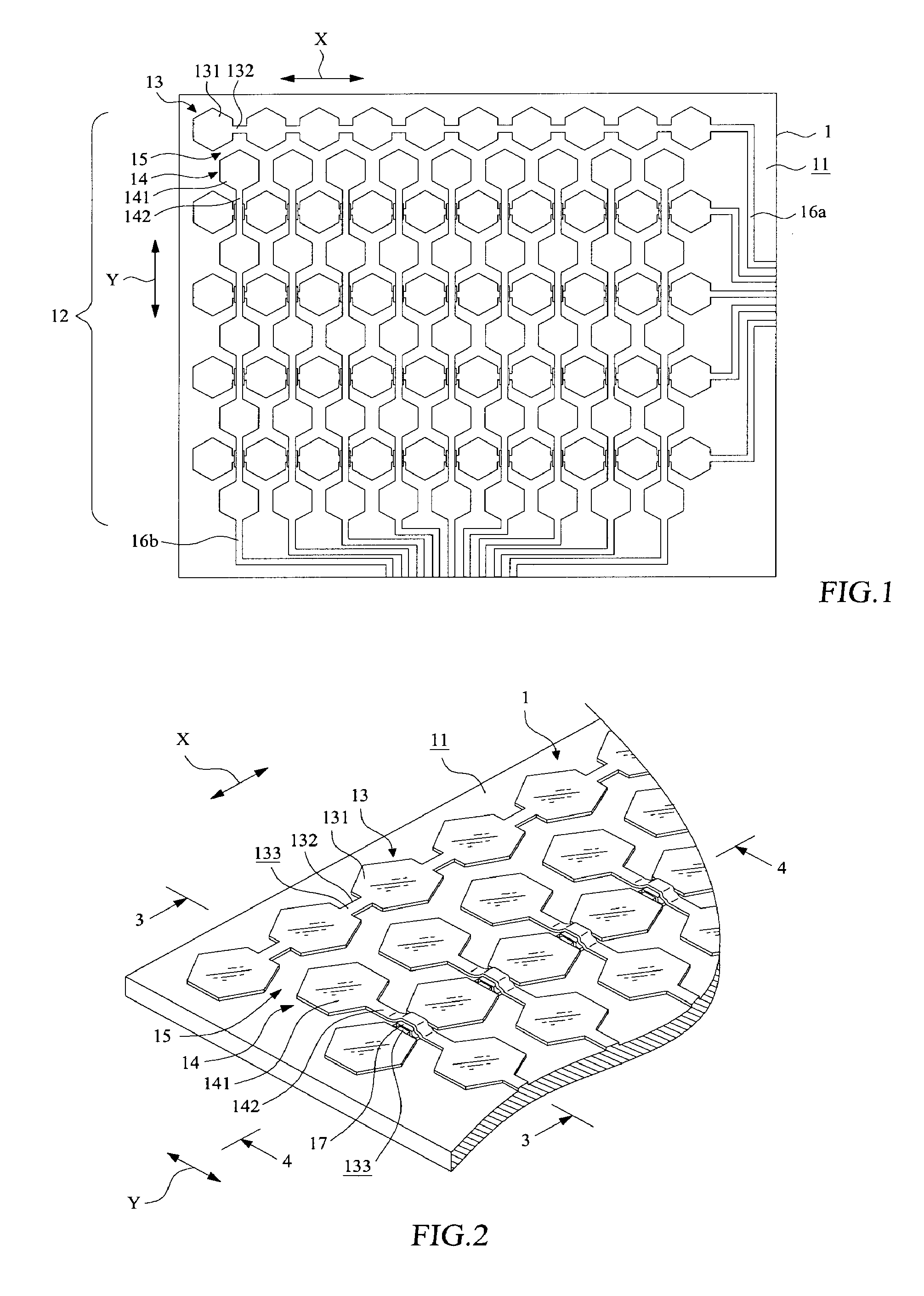
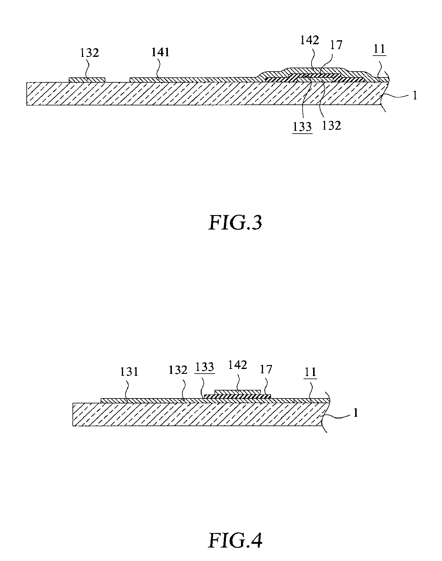
[0030]With reference to the drawings and in particular to FIGS. 1 and 2, of which FIG. 1 illustrates a plan view of a conductor pattern structure of a capacitive touch panel in accordance with the present invention and FIG. 2 illustrates a perspective view of a portion of the conductor pattern structure of the capacitive touch panel, generally designated with reference numeral 12, is formed on a surface 11 of a substrate 1. The conductor pattern structure 12 comprises a plurality of conductor assemblies 13 extending along a first axis, which will be referred to as “first-axis conductor assemblies”, and a plurality of conductor assemblies 14 extending along a second axis, which will be referred to as “second-axis conductor assemblies”. Each of the first-axis conductor assemblies 13 is parallel to other first-axis conductor assemblies 13, and each of the second-axis conductor assemblies 14 is parallel to other second-axis conductor assemblies 14. The first-axis conductor assemblies 13...

second embodiment

[0044]In the embodiment discussed previously, the first-axis conductor cells and the second-axis conductor cells are each formed on the substrate in an array form to constitute the conductor pattern structure of the capacitive touch panel. Based on the same philosophy, a small number of conductor cells can also be used to construct a conductor pattern structure of the capacitive touch panel. This is illustrated in FIG. 10 as the disclosure, wherein two adjacent first-axis conductor cells 31, 32 are formed on a surface 21 of a substrate 2 and a signal transmission line 34 is connected to the conductor cell 32. A first-axis conduction line 33 connects between the adjacent first-axis conductor cells 31, 32. An insulation layer 4 is formed on a surface of the first-axis conduction line 33.

[0045]Along an axis that is different from the first-axis conductor cells 31, 32, two adjacent second-axis conductor cells 51, 52 are arranged and a second-axis conduction lines 53 connects between the...


PUM

PropertyMeasurementUnit
transparentaaaaaaaaaa
capacitanceaaaaaaaaaa
transparencyaaaaaaaaaa

Abstract

Disclosed is a conductor pattern structure of a capacitive touch panel. First-axis conductor assemblies and second-axis conductor assemblies are formed on a surface of a substrate. Each first-axis conductor assembly includes a plurality of first-axis conductor cells that are interconnected by first-axis conduction lines. An insulation layer is formed on a surface of each first-axis conduction line. Each second-axis conductor assembly includes a plurality of second-axis conductor cells that are interconnected by second-axis conduction lines. Each second-axis conduction line extends across the insulation layer of the associated first-axis conduction line.

Description

FIELD OF THE INVENTION[0001]The present invention relates to the field of touch panel devices, and in particular to a conductor pattern structure of a capacitive touch panel.BACKGROUND OF THE INVENTION[0002]Touch panels have been of wide applications in the fields of household appliances, communications, and electronic information appliances. An example of the common applications of the touch panel is an input interface of a personal digital assistant (PDA), an electrical appliance, or a game machine, etc. The current trend of integration of a touch panel and a display panel allows a user to use his or her finger or a stylus to point a control icon shown on the panel in order to execute a desired function on a PDA, an electrical appliance or a game machine, etc. The touch panel is also applied in a public information inquiry system to provide an efficient operation system for the public.[0003]A conventional touch panel comprises a substrate having a surface on which sensing zones ar...

Claims


Application Information

Patent Timeline
Patent Type & Authority Applications(United States)
IPC IPC(8): G06F3/041
CPCG06F1/169G06F3/044Y10T29/49004G06F2203/04111G06F1/1692G06F3/0443G06F3/0446G06F2203/04103G06F3/04164
Inventor CHANG, CHING-YANGCHIEN, SHUN-TA
Owner TRENDON TOUCH TECHNOLOGY CORPORATION
Why Eureka
Try Eureka