Self-aligned bit line under word line memory array

a memory array and self-aligning technology, applied in semiconductor devices, digital storage, instruments, etc., can solve the problems of imposing footprint limitations and limiting factors in the footprin

Active Publication Date: 2011-12-15
IBM CORP +1
View PDF7 Cites 51 Cited by
  • Summary
  • Abstract
  • Description
  • Claims
  • Application Information

AI Technical Summary

Benefits of technology

[0008]A memory device is described that comprises a plurality of bit lines and an array of vertical transistors arranged on the plurality of bit lines. A plurality of word lines is formed along rows of vertical transistors in the array which comprise thin film sidewalls of word line material and are arranged so that the thin film sidewalls merge in the row direction, and do not merge in the column direction, to form word lines. The word lines provide “surrounding gate” structures for embodiments in which t

Problems solved by technology

In programmable resistance devices, a limiting factor in the footprint can be the layout of access devices used in the array to select individual cells.
However, limit

Method used


Image

  • Self-aligned bit line under word line memory array
  • Self-aligned bit line under word line memory array
  • Self-aligned bit line under word line memory array

Examples


Embodiment Construction

[0033]A detailed description of embodiments of the technology described herein is provided with reference to FIGS. 1-24.

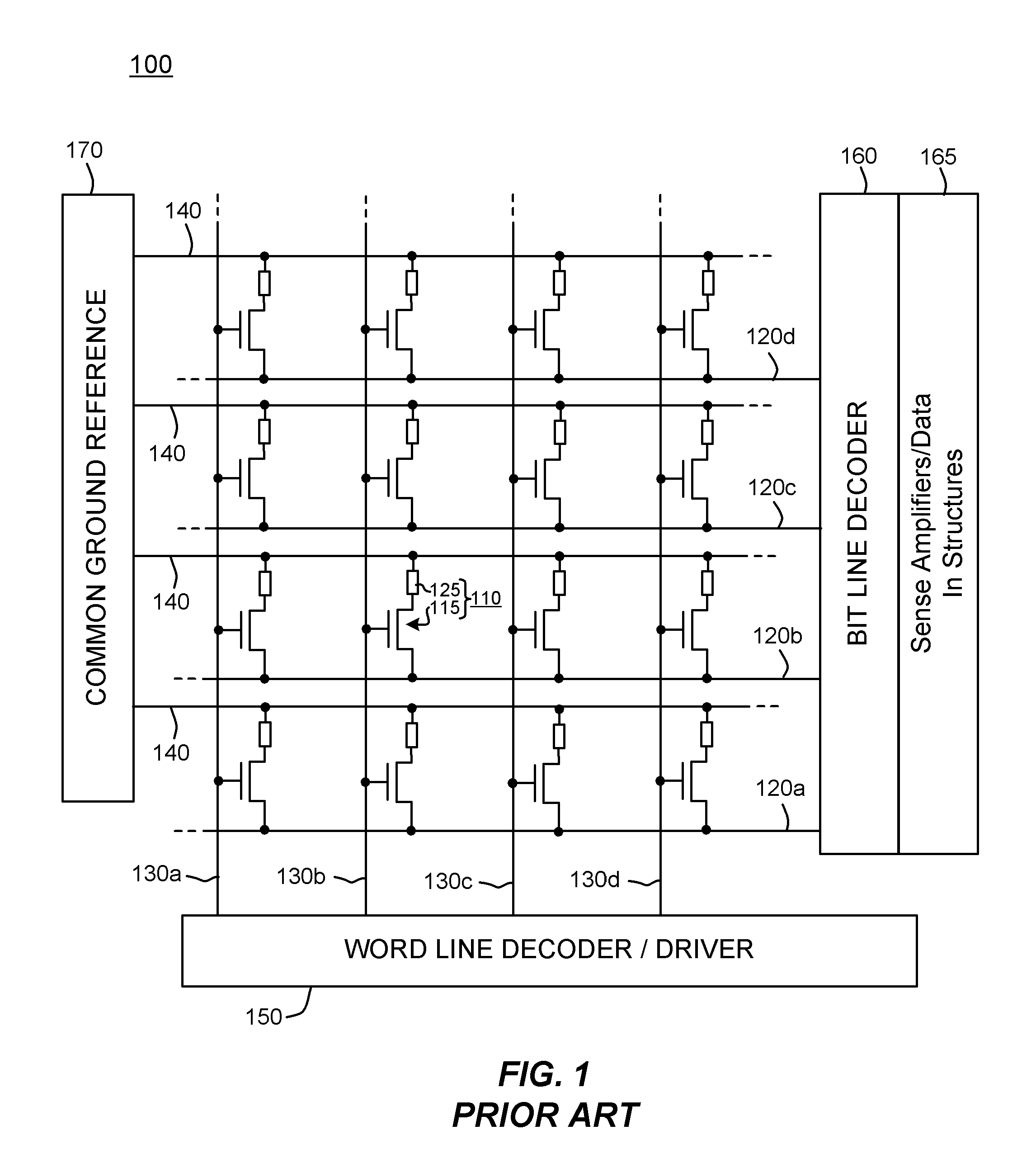
[0034]FIG. 1 is a schematic diagram of a portion of a memory cell array 100 implemented using programmable resistance memory cells, as is typical of prior art integrated circuit memory designs. The array 100 comprises a plurality of bit lines 120a-120d extending in parallel in a first direction and in electrical communication with bit line decoder 160. A plurality of word lines 130a, 130b, 130c, 130d extend in parallel in a second direction and are in electrical communication with word line decoder / driver 150. In the schematic diagram of FIG. 1, each of the memory cells (e.g. memory cell 110) of array 100 includes a field effect transistor access device (e.g. transistor 115) and a memory element (e.g. element 125) arranged in electrical series between a bit line (e.g. 120b) via a memory plane 140 (represented by horizontal lines in this illustration) and a common g...


PUM


Abstract

A memory device is described that comprises a plurality of bit lines and an array of vertical transistors arranged on the plurality of bit lines. A plurality of word lines is formed along rows of vertical transistors in the array which comprise thin film sidewalls of word line material and arranged so that the thin film sidewalls merge in the row direction, and do not merge in the column direction, to form word lines. The word lines provide “surrounding gate” structures for embodiments in which the vertical transistors are field effect transistors. Memory elements are formed in electrical communication with the vertical transistors. A fully self-aligned process is provided in which the word lines and memory elements are aligned with the vertical transistors without additional patterning steps.

Description

PARTIES TO A JOINT RESEARCH AGREEMENT[0001]International Business Machines Corporation, a New York Corporation, and Macronix International Corporation, Ltd., a Taiwan corporation, are parties to a Joint Research Agreement.BACKGROUND OF THE INVENTION[0002]1. Field of the Invention[0003]The present invention relates to high density memory devices based on phase change memory materials, like chalcogenides, and on other programmable resistance materials, and methods for manufacturing such devices.[0004]2. Description of Related Art[0005]Phase-change-based memory materials, like chalcogenides and similar materials, can be caused to change between an amorphous phase and a crystalline phase by application of electrical current at levels suitable for implementation in integrated circuits. The generally amorphous phase is characterized by higher electrical resistivity than the generally crystalline phase, which can be readily sensed to indicate data. These properties have generated interest ...

Claims


Application Information

Patent Timeline
IPC IPC(8): G11C11/00H01L45/00H01L21/82
CPCH01L27/2445H01L27/2454H01L27/2472H01L45/06H01L45/085H01L45/148H01L45/142H01L45/144H01L45/146H01L45/147H01L45/1233
Inventor LUNG, HSIANG-LANLAM, CHUNG HONLAI, ERH-KUNBREITWISCH, MATTHEW J.
Owner IBM CORP
Why Eureka
Try Eureka