Fringe field switching (FFS) liquid crystal display (LCD) panel, manufacturing method thereof and LCD

A liquid crystal display panel and fringe field switch technology, which is applied in semiconductor/solid-state device manufacturing, instruments, electric solid-state devices, etc., can solve the problem that the transmittance of the pixel electrode 14 cannot be significantly improved, and achieve the reduction of driving voltage and voltage reduction. Poor, the effect of improving the transmittance

Active Publication Date: 2011-03-30
KUSN INFOVISION OPTOELECTRONICS
View PDF3 Cites 50 Cited by
  • Summary
  • Abstract
  • Description
  • Claims
  • Application Information

AI Technical Summary

Problems solved by technology

Figure 5 and image 3 was carried out under the same simulation conditions, by Figure 5 It can be seen that the electric field still mainly exists at the slanted edge of the pixel electrode 14, therefore, the transmittance above the pixel electrode 14 cannot be significantly improved, and this kind of FFS type liquid crystal display panel with electrode protrusions still has the above-mentioned problems. technical problem

Method used


Image

  • Fringe field switching (FFS) liquid crystal display (LCD) panel, manufacturing method thereof and LCD
  • Fringe field switching (FFS) liquid crystal display (LCD) panel, manufacturing method thereof and LCD
  • Fringe field switching (FFS) liquid crystal display (LCD) panel, manufacturing method thereof and LCD

Examples


Embodiment Construction

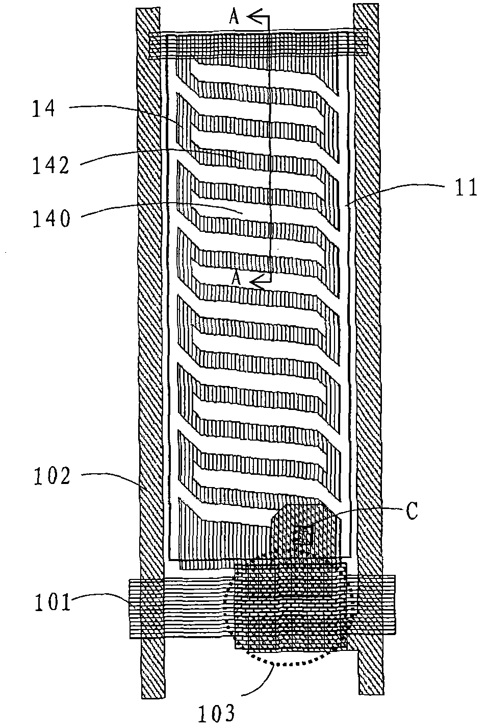
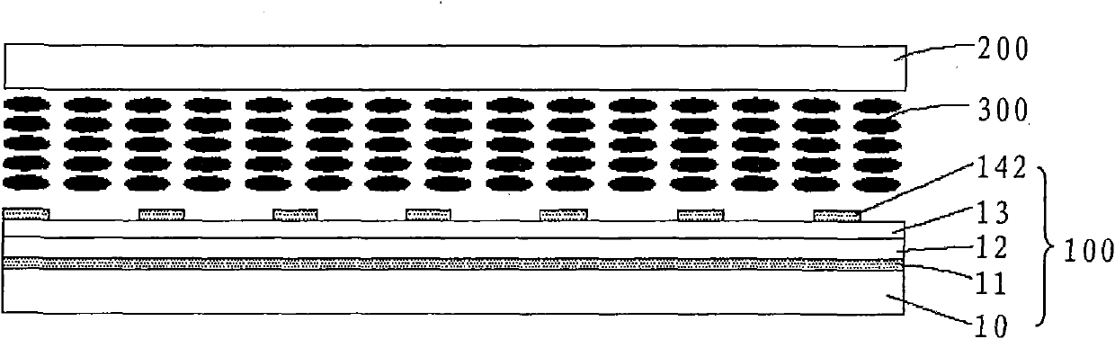
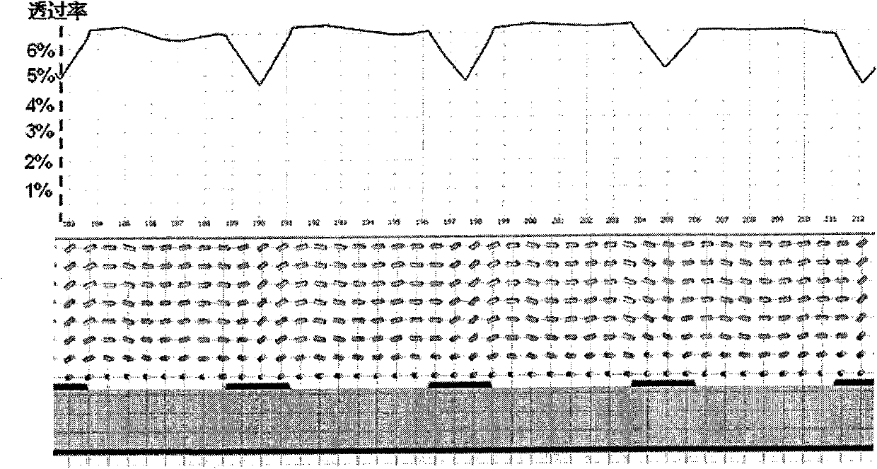
[0037] In order to make the above objects, features and advantages more comprehensible, specific implementations of the present invention will be described in detail below in conjunction with the accompanying drawings.

[0038] When describing the embodiments of the present invention in detail, for the convenience of explanation, the cross-sectional view showing its structure is not partially enlarged according to the general scale, and the schematic diagram is only an example, which should not limit the protection scope of the present invention. In addition, the three-dimensional space dimensions of length, width and depth should be included in actual production.

[0039] The liquid crystal display of the present invention includes a fringe field switching (Fringe Field Switching, FFS) type liquid crystal display panel and a driving circuit (not shown) connected to the FFS type liquid crystal display panel.

[0040] In addition, it should be noted that, for the sake of clarit...


PUM

PropertyMeasurementUnit
heightaaaaaaaaaa
widthaaaaaaaaaa

Abstract

The invention discloses a fringe field switching (FFS) liquid crystal display (LCD) panel, a manufacturing method thereof and an LCD. The LCD panel comprises a thin film transistor (TFT) array substrate, and the TFT array substrate comprises a transparent substrate as well as a plurality of scanning lines and a plurality of data lines which are formed on the transparent substrate, wherein, the plurality of scanning lines are crossed with the plurality of data lines to limit a plurality of pixel regions; each pixel region comprises a first transparent electrode, a second transparent electrode and a TFT; the first transparent electrode is equipped with a plurality of strip slots so that a plurality of first strip transparent electrode parts which are respectively spaced by the plurality of strip slots and electrically connected with each other are formed on the first transparent electrode; and each pixel region further comprises a plurality of strip projections which are positioned below the second transparent electrode and are corresponding to the positions of the plurality of slots of the first transparent electrode. The invention has the advantages that the driving voltage of theLCD panel can be lowered and the transmissivity can be improved.

Description

technical field [0001] The present invention relates to the field of thin film transistor liquid crystal display (TFT-LCD), in particular to a fringe field switching (Fringe Field Switching, FFS) type liquid crystal display panel and a manufacturing method thereof, and a liquid crystal display device having the fringe field switching type liquid crystal display panel. Background technique [0002] At present, TFT-LCD occupies a dominant position in the field of flat panel display and has been widely used in various fields. The traditional twisted nematic (Twisted Nematic, TN) liquid crystal display panel has the problem of narrow viewing angle. In order to realize the liquid crystal display with wide viewing angle, the In-Plane Switching (IPS) liquid crystal display FFS type liquid crystal display panels have been developed. Compared with IPS type liquid crystal display panels, FFS type liquid crystal display panels have the advantages of wide viewing angle and high transmit...

Claims


Application Information

Patent Timeline
Patent Type & Authority Applications(China)
IPC IPC(8): G02F1/1343G02F1/1362G02F1/1333H01L27/12H01L21/77
Inventor 钟德镇孔祥建廖家德戴文君
Owner KUSN INFOVISION OPTOELECTRONICS
Why Eureka
Try Eureka