

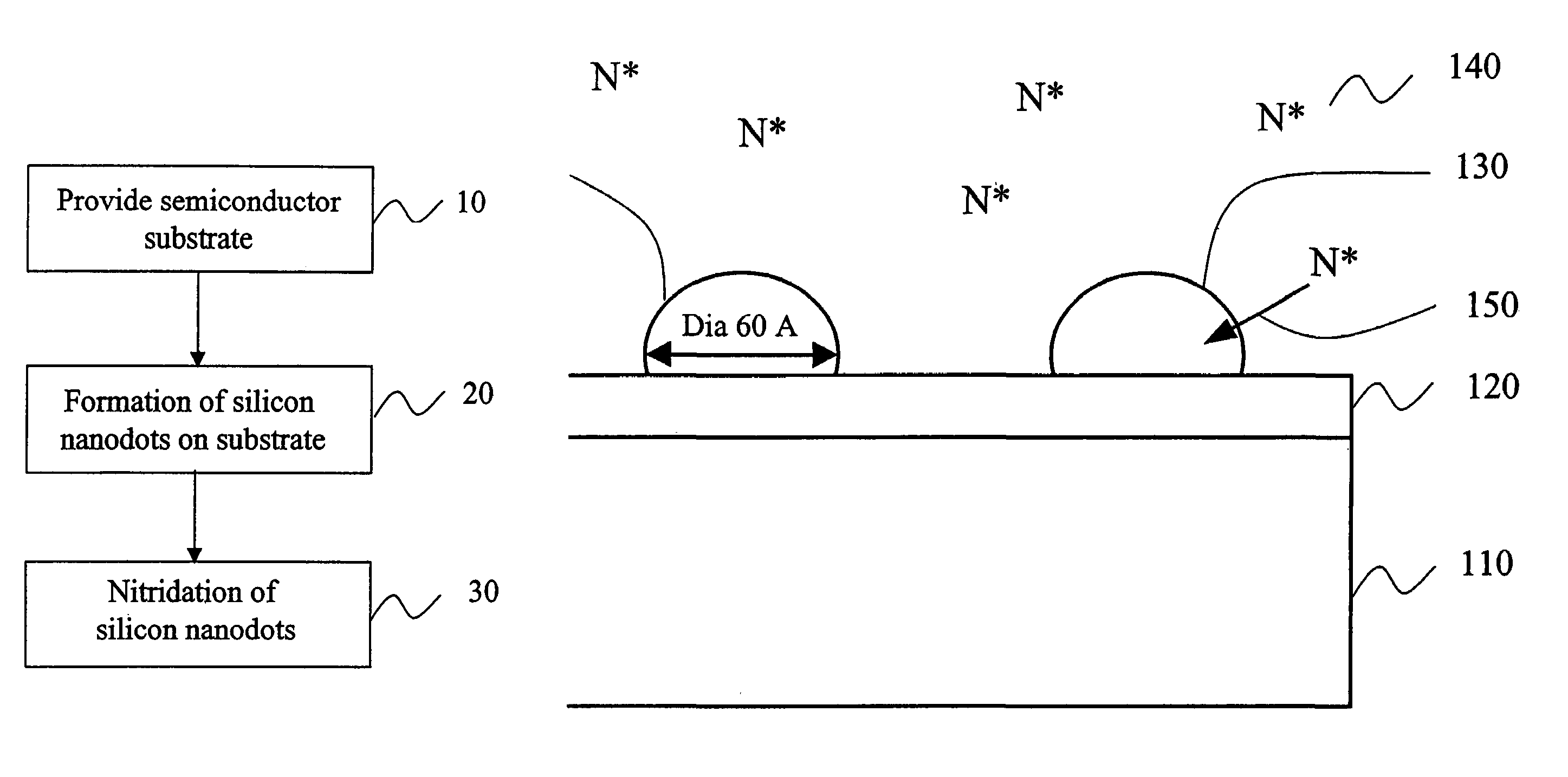
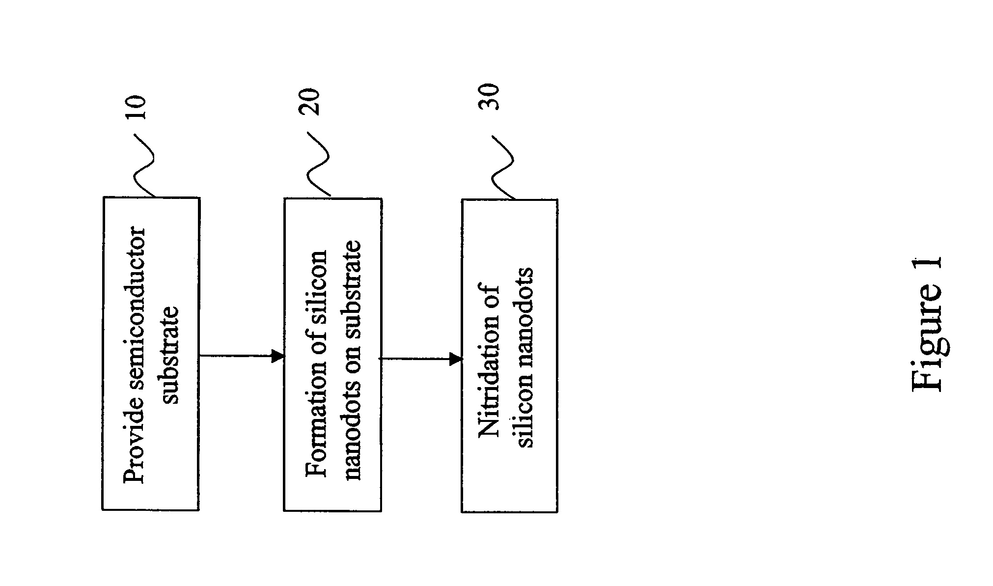
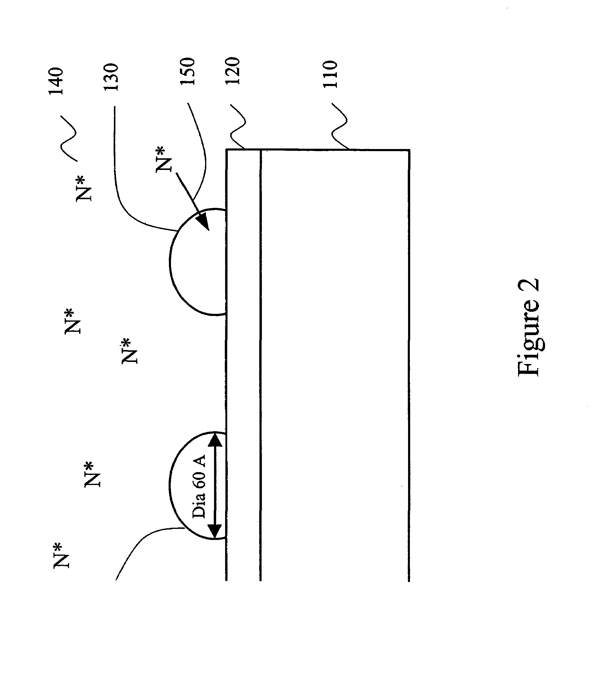
Method of fabricating silicon nitride nanodots
a silicon nitride nanodot and nanodot technology, applied in the field of semiconductor manufacturing, can solve the problems of increasing the risk of defects occurring in the tunnel oxide, the charge retention characteristics of the device are very sensitive to the presence or absence, and the further scaling down presents serious problems, so as to achieve the effect of easy implementation in the production environmen
- Summary
- Abstract
- Description
- Claims
- Application Information
AI Technical Summary
Benefits of technology
Problems solved by technology
Method used
Image

Examples
example
Synthesis of Nitride Nanodots
[0030]Silicon substrates were subjected to an ultra diluted wet oxidation process as described in U.S. patent application Ser. No. 09 / 723,323 of applicant to form a 2 nm thick layer of oxide. The low pressure chemical vapor deposition “LPCVD” seed process was carried out in a LPCVD vertical furnace from ASM, model A400™-XT, (ASM International N.V., Bilthoven, The Netherlands), designed for 200 mm wafers with a usable load size of 150 wafers. The temperature was 540° C., the pressure 550 mTorr, SiH4 flow 20 sccm, nitrogen carrier flow 1 slm and exposure time 10 min.
[0031]The surface of this exemplary sample, after silicon nanodot formation and prior to nitridation, was studied by scanning electron microscopy (SEM) and is shown in FIG. 4. The resulting average nanodot size was 6 nm. It will be clear to one of skill in the art that the size of the nanodots can easily be adjusted by adjusting the deposition time or seed time.
[0032]The nitridation was perform...
PUM
 Abstract
Description
Claims
Application Information