Electrooptic device, method for manufacturing the same, and electronic apparatus

a technology of electronic equipment and liquid crystal devices, applied in non-linear optics, identification means, instruments, etc., can solve the problems of reducing reliability of liquid crystal devices, increasing the significance of problems described above, and prone to corrosion of wires, so as to reduce manufacturing costs and simplify manufacturing steps. , the effect of further reducing the manufacturing cos

Inactive Publication Date: 2005-11-29
SEIKO EPSON CORP
View PDF31 Cites 7 Cited by
  • Summary
  • Abstract
  • Description
  • Claims
  • Application Information

AI Technical Summary

Benefits of technology

[0041]According to the method described above, compared to the case in which the thin-film diodes and the wires are formed independently of each other by different steps, the manufacturing cost can be reduced and the manufacturing steps can be simplified.
[0042](17) The method for manufacturing the electrooptic device described above may further comprise a step of forming pixel electrodes, which are provided on the first substrate and which are connected to the second metal films of the thin-film diodes; and a third wire layer forming step of, prior to the bonding step, forming third wire layers, which form the wires, in the region overlapping the sealing material and the outside region thereof of the first substrate. In the method described above, the third wire layers are preferably formed by the same layer as that for the pixel electrodes at the same time as the pixel electrodes are formed. According to the method described above, the manufacturing cost can be further reduced.

Problems solved by technology

However, since wires formed on the protruding region are exposed to outside air, moisture or the like in the outside air is likely to adhere to the wires, and hence, the wires are liable to corrode.
In addition, when corrosion of the wires occurs as described above, the conduction between the wires and the surface-mount components described above becomes insufficient, and as a result, a problem may arise in that the reliability as the liquid crystal device is degraded.
On the other hand, when decrease in wiring resistance of the wires is considered, the wires are preferably formed of a low resistance metal such as aluminum or chromium; however, since these metals have high ionicity and are susceptible to corrosion, the problem described above becomes more significant.

Method used


Image

  • Electrooptic device, method for manufacturing the same, and electronic apparatus
  • Electrooptic device, method for manufacturing the same, and electronic apparatus
  • Electrooptic device, method for manufacturing the same, and electronic apparatus

Examples


first embodiment

[0064](First Embodiment of Electrooptic Device)

[0065]Hereinafter, an embodiment of the present invention will be described with reference to the case in which the present invention is applied to a liquid crystal device which is an active matrix type provided with TFD (Thin Film Diode) elements as a switching element, uses liquid crystal as an electrooptic material, and is a reflective type using external light such as sunlight or indoor light.

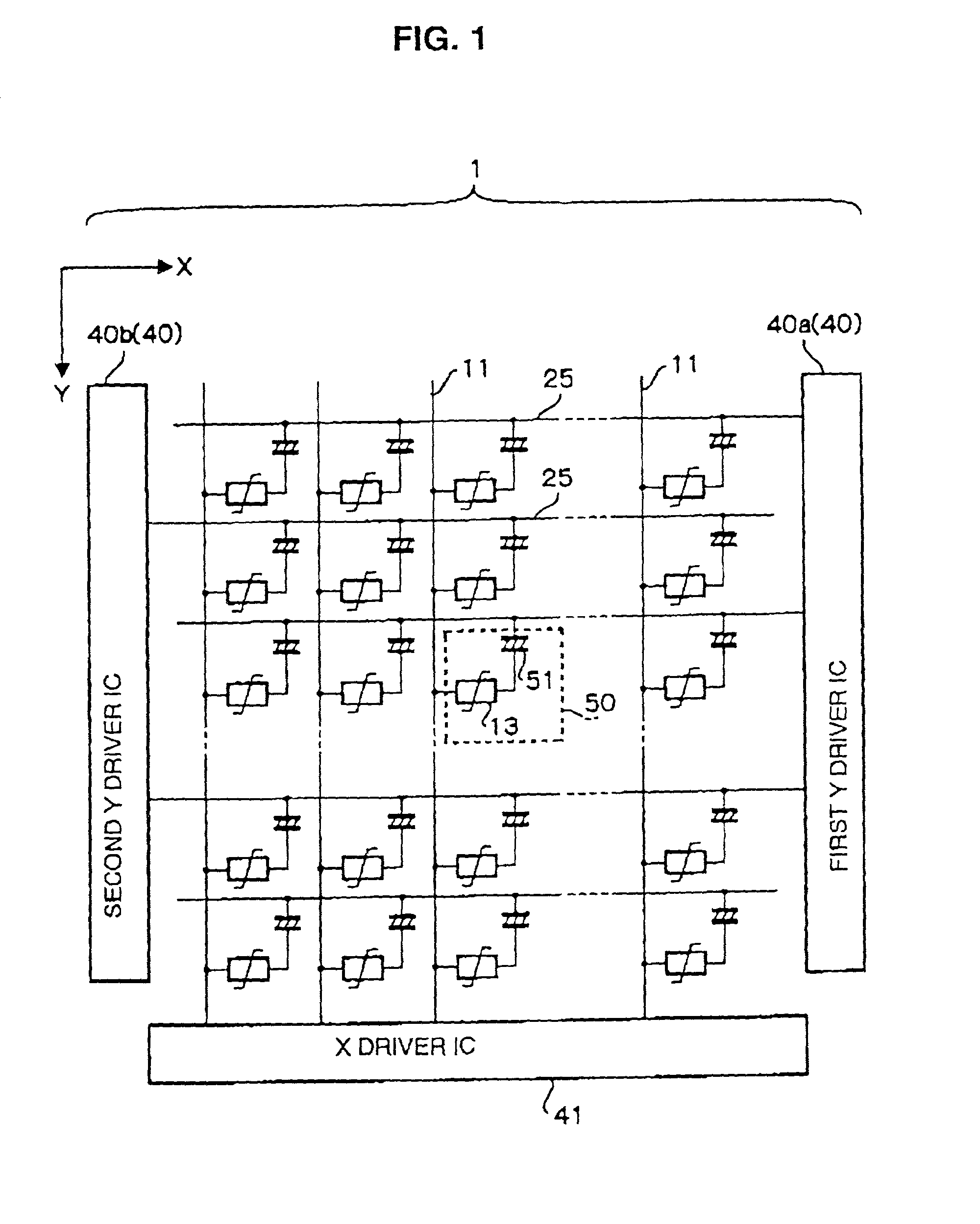
[0066]FIG. 1 is a block diagram showing the electrical structure of the liquid crystal device of this embodiment. As shown in this figure, a liquid crystal device 1 comprises a plurality of scanning lines 25 extending in the X direction, a plurality of data lines 11 extending in the Y direction perpendicular to the X direction, a plurality of display dots 50 provided at the intersections between the scanning lines 25 and the data lines 11. Each display dot 50 has the structure in which a liquid crystal display element 51 and a TFD element 13 ar...

embodiment

[0117](Embodiment of Method for Manufacturing Electrooptic Device)

[0118]Next, a method for manufacturing an electrooptic device will be described. First, methods for manufacturing individual elements, such as the data lines 11, the TFD elements 13, and the like, which are provided on the element substrate 10 shown in FIG. 3, will be described. In FIGS. 9 and 10, a method for manufacturing one display dot 50 on the element substrate 10 is sequentially shown by steps. In addition, in FIG. 11, a method for manufacturing wires 16 is sequentially shown by steps.

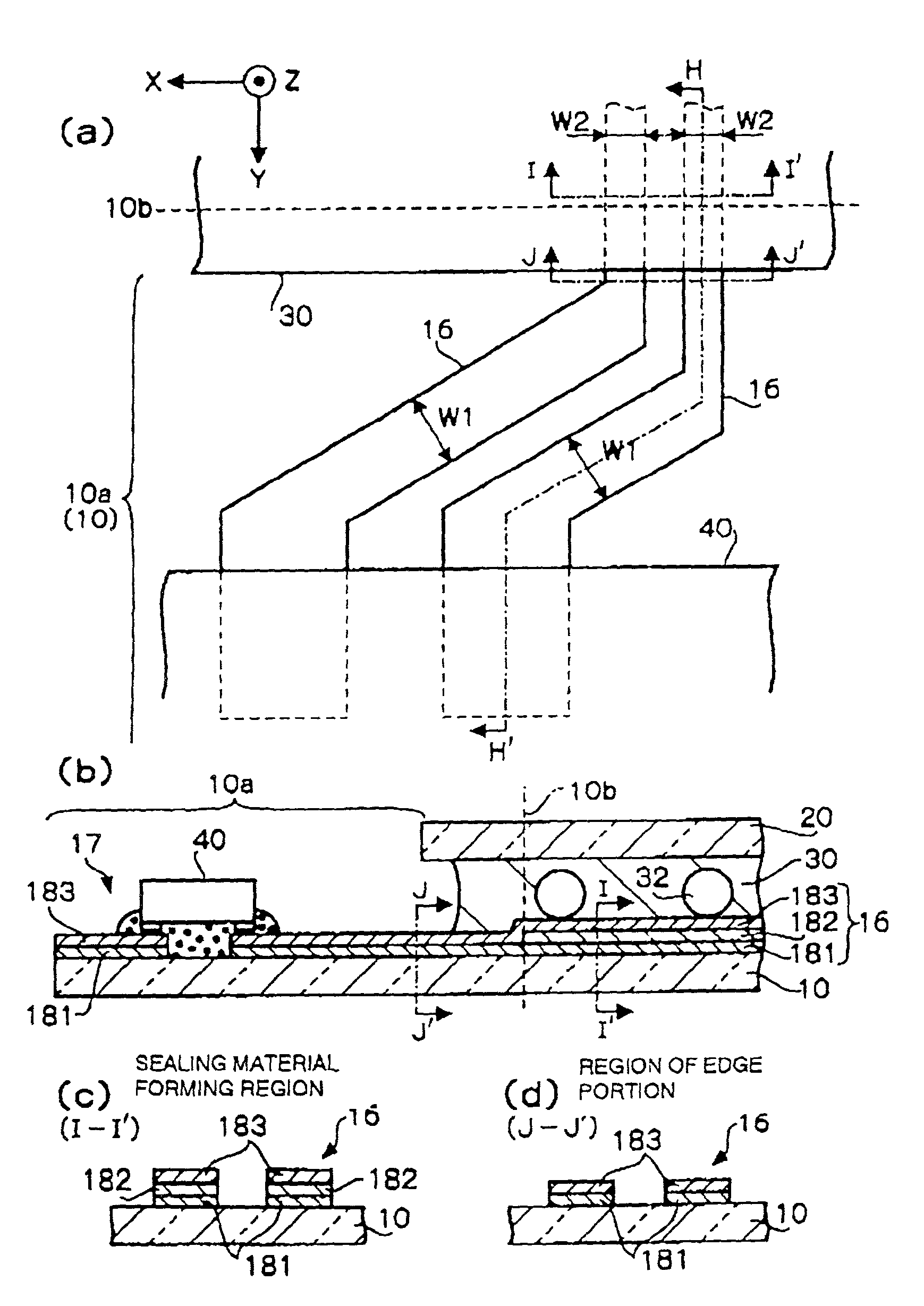
[0119]As described above, the wire 16 in this embodiment is formed of the same layers as those for the TFD element 13 and the pixel electrode 12. Accordingly, hereinafter, methods for manufacturing the display dot 50 and the wire 16 will both be described. In addition, concerning the regions shown in FIG. 6 in which the wires 16 are to be formed, the positional relation among the protruding region 10a, the region in which the seal...

second embodiment

[0145](Second Embodiment of Electrooptic Device)

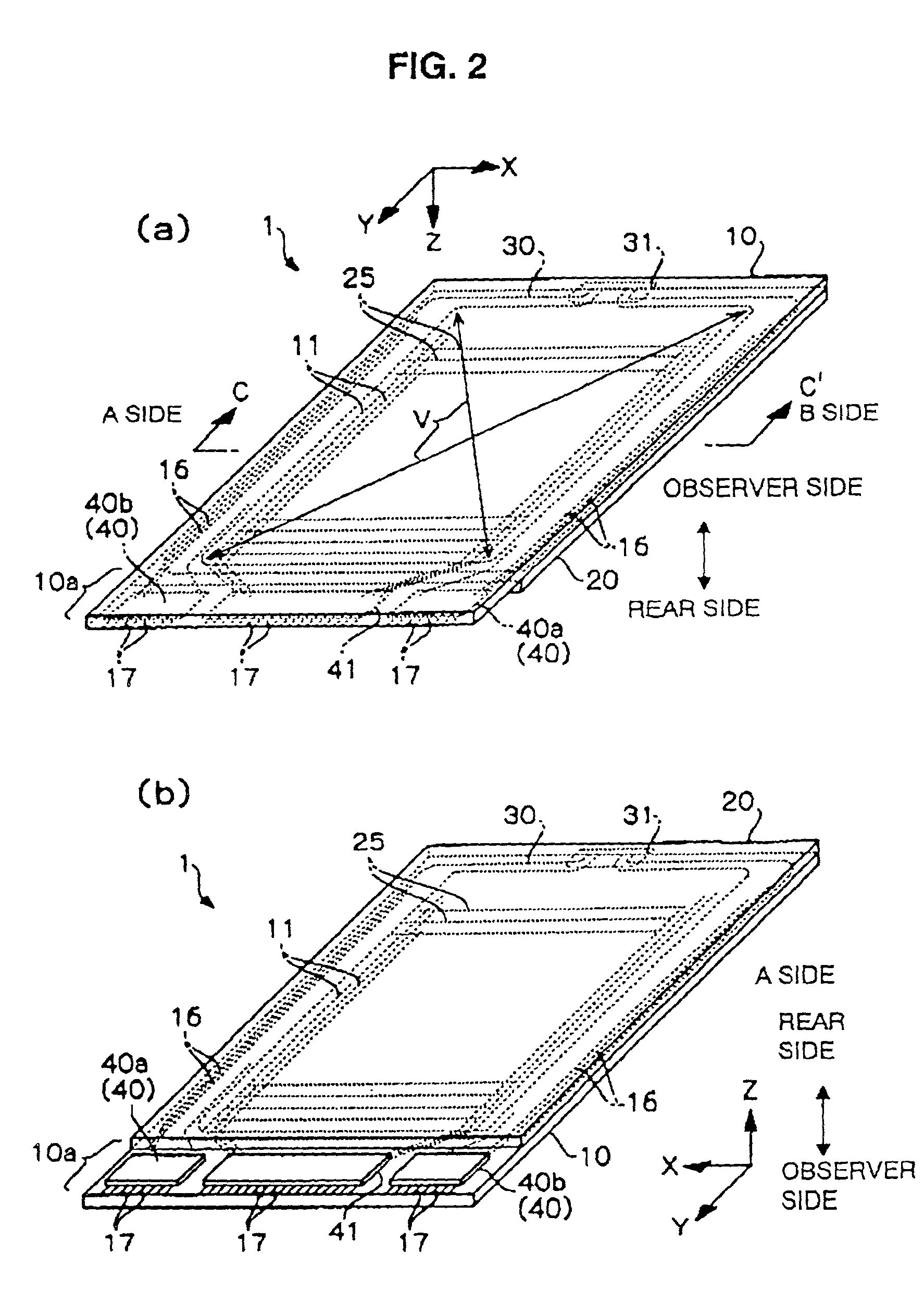
[0146]In the embodiment shown in FIG. 6, the part of the wire 16 is covered with one side of the sealing material 30 extending in the direction approximately equivalent to that of the part mentioned above; however, instead of that mentioned above, the structure shown in FIG. 14 may also be used. In FIG. 14, the wire configuration is shown when a liquid crystal device 81 is viewed from the observer side. In addition, the same reference numerals in FIG. 6 designate the same constituent elements in FIG. 14. In FIG. 14, as is the case in FIG. 6, the element substrate 10 is disposed at the front position of the plane and the other elements are disposed at the rear side with respect to the element substrate 10.

[0147]In FIG. 14, the wires 16 are formed on the element substrate 10 and are each composed of the conduction portion 16a and the extension portion 16b. The position at which the conduction portion 16a is connected to the conduction po...


PUM

PropertyMeasurementUnit
thicknessaaaaaaaaaa
thicknessaaaaaaaaaa
thicknessaaaaaaaaaa

Abstract

An electrooptic device has a first substrate 10 and a second substrate 20 disposed to oppose each other, and liquid crystal 35 provided between the first substrate 10 and the second substrate 20. This electrooptic device has a sealing material 30 surrounding the liquid crystal 35 and wires 16 continuously extending along one side of the first substrate 10 to another side intersecting said one side. The wires 16 each have a first wire layer which is continuously formed in the inside region of the sealing material 30 and the outside region of the sealing material 30 or which is continuously formed in the region overlapping the sealing material 30 and the outside region of the sealing material 30; and a second wire layer 182 which is formed in the inside region of the sealing material 30 or the region overlapping the sealing material 30. Since being not exposed to outside air, the second wire layer 182 is not corroded.

Description

BACKGROUND OF THE INVENTION[0001]1. Technical Field of the Invention[0002]The present invention relates to electrooptic devices, such as a liquid crystal device, an EL (Electro Luminescent) device, and an electrophoretic device, to methods for manufacturing the electrooptic devices, and to electronic apparatuses provided with these electrooptic devices.[0003]2. Description of the Related Art[0004]In recent years, in electronic apparatuses such as mobile phones, portable information terminal apparatuses, and personal computers, liquid crystal devices have been widely used as, for example, a display portion for displaying information. In addition, it has been considered that an EL device will also be used in the future.[0005]The liquid crystal device described above generally comprises a pair of substrates bonded together with a sealing material provided therebetween, liquid crystal enclosed between the substrates, and electrodes applying a voltage to the liquid crystal. In addition, ...

Claims


Application Information

Patent Timeline
Patent Type & Authority Patents(United States)
IPC IPC(8): G02F1/1339G02F1/1333G02F1/1345G02F1/1362G02F1/1365G09F9/00G09F9/30
CPCG02F1/136286G02F1/1345G02F2001/133388G02F2001/13629G02F1/133388G02F1/13629
Inventor TANAKA, CHIHIROTSUYUKI, TADASHIKANEKO, HIDEKI
Owner SEIKO EPSON CORP
Why Eureka
Try Eureka