

Barrier first method for single damascene trench applications
- Summary
- Abstract
- Description
- Claims
- Application Information
AI Technical Summary
Benefits of technology
Problems solved by technology
Method used
Image


Examples
implementation example
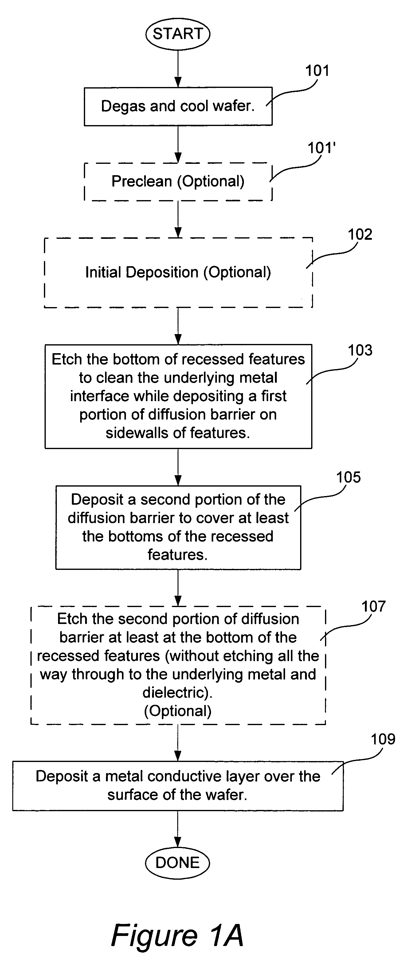
[0052]As mentioned, methods of the invention employ a simultaneous etch / deposition to etch barrier material at the trench bottom while depositing barrier material elsewhere on a wafer substrate. As well, various aspects of process flows involve deposition of barrier materials (by ALD, CVD, PDL or PVD), precleaning, and degassing operations. In preferred embodiments all these process steps are done in the same processing tool. Tools that allow degas, preclean, ALD, PDL, or CVD deposition, and PVD deposition all under the same vacuum are the INOVA and INOVA xT deposition systems available from Novellus Systems of San Jose, Calif. These systems are comprised of processing modules, e.g., for Degas, Cool, Preclean, PVD, CVD, PDL or ALD processes, mounted to the same wafer handling system. Therefore, once a wafer is in the tool and a vacuum is established, all of the above described process aspects are performed without breaking vacuum. For example, a wafer is placed into the system, it i...
PUM
 Abstract
Description
Claims
Application Information