Method for manufacturing porous structure and method for forming pattern

a technology of porous structure and pattern, which is applied in the manufacture of electronic systems, magnetic recording, record information storage, etc., can solve the problems of no other choice to form fine patterns, no other choice, and low manufacturing cost, and achieves high process throughput and considerable regularity.

Inactive Publication Date: 2006-08-29
KK TOSHIBA
View PDF24 Cites 48 Cited by
  • Summary
  • Abstract
  • Description
  • Claims
  • Application Information

AI Technical Summary

Benefits of technology

[0008]An object of the present invention is to provide a pattern forming material and a method for forming a pattern, which show high process throughput and capable of forming very easily a planar pattern or three-dimensional structure of the order of nanometers having considerable regularity.
[0009]A still another object of the present invention is to provide a method for manufacturing easily a magnetic recording medium, a field emission display, a field emission cathode, a separator and electrode for an electrochemical cell, a catalytic electrode for a fuel cell, a filter, etc., by making use of the aforementioned material.

Problems solved by technology

Lithography is employed in these processes, and thus the manufacturing cost becomes higher as more micro-fabrications are needed.
However, a simple patterning method has not known hitherto, there is no other choice to form a fine pattern by lithography using an electronic beam or deep ultraviolet ray in such a technical field.
As mentioned above, in the lithography technique, operations are complicated and enormous investment is required as the processing dimension becomes smaller.
However, the ozonation is complicated as well as needs relatively long reaction time, so that it is difficult to improve throughput.
Also, since the osmium oxide has high level of toxicity, it is scarcely used in general purpose from the viewpoint of safety.

Method used


Image

  • Method for manufacturing porous structure and method for forming pattern
  • Method for manufacturing porous structure and method for forming pattern
  • Method for manufacturing porous structure and method for forming pattern

Examples


examples

[0293]Hereinafter, the present invention will be specifically described based on examples. It should be noted that the present invention is not limited to these examples.

synthesis example

[0294]A diblock copolymer (1) of polystyrene (PS) and polymethyl methacrylate (PMMA) is synthesized by living anion polymerization. Molecular sieves and activated alumina are added to polystyrene monomer and polymethyl methacrylate monomer, respectively, followed by leaving to stand for two days to remove water and an inhibitor. These monomers are distilled under reduced pressure, and then the atmosphere is replaced with argon gas. Dehydrated THF (Wako Junyaku Co., Ltd.) is prepared as a reaction solvent to which metallic sodium is added as a dehydrating agent, and then reflux is performed for two days. As a polymerization initiator, sec-butyl lithium (Kanto Kagaku Co., Ltd.) is employed.

[0295]As a polymerization apparatus, a pressure reactor (Taiatsu Glass Co., Ltd.) is employed. The reaction is carefully performed under a pressurized argon atmosphere of 4 atm so as to prevent outside air from entering the reaction system. While flowing argon, the dehydrated THF and polymerization ...

example 1

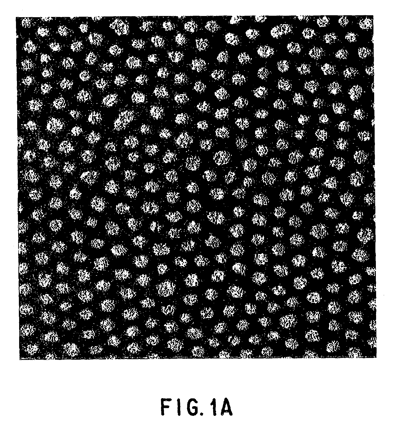
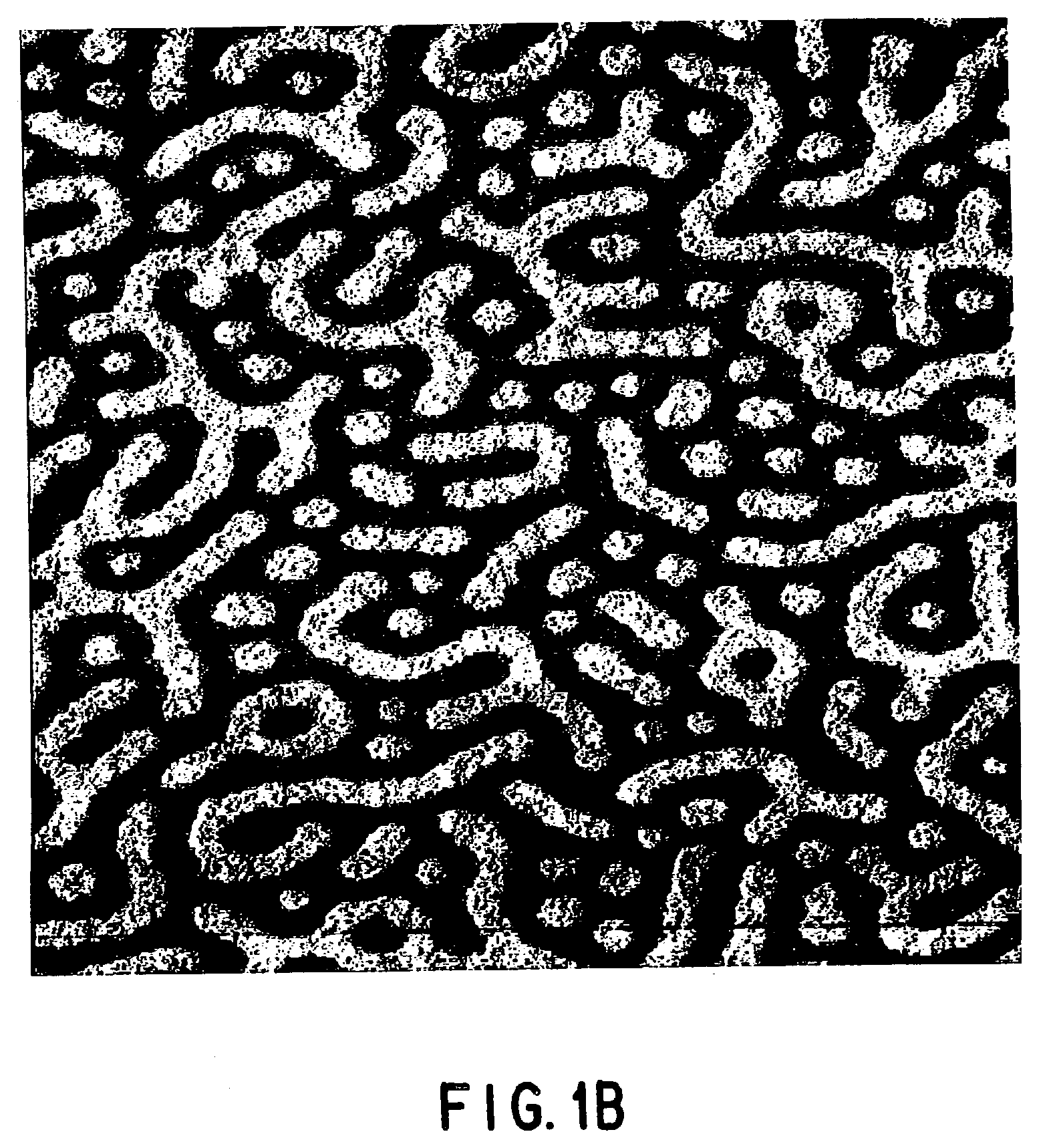
[0298]Two wt % of the diblock copolymer (1) is dissolved in propylene glycol monoethyl ether acetate (PGMEA), followed by filtering the solution, and then an SiO substrate is spin-coated with the solution at 2,500 rpm. The substrate is heated to 110° C. for 90 seconds to evaporate the solvent. Thereafter, the substrate is placed in an oven, and annealing is performed in a nitrogen atmosphere at 210° C. for 10 minutes, subsequently at 135° C. for 10 hours. Since the temperature of 210° C. is just below a temperature that decomposition of the acrylic block takes place, the short time annealing enables to flatten the film with dissipating hysteresis after spin-coating. Further, the annealing at the temperature of about 135° C. enables to promote microphase separation of the diblock copolymer efficiently, so that a film having micro polymer phases is formed.

[0299]Reactive ion etching (RIE) is performed to the sample under the conditions of CF4, 0.01 Torr, 150 W of progressive wave, and ...


PUM

PropertyMeasurementUnit
molecular weight distributionaaaaaaaaaa

Abstract

A pattern forming material contains a block copolymer or graft copolymer and forms a structure having micro polymer phases, in which, with respect to at least two polymer chains among polymer chains constituting the block copolymer or graft copolymer, the ratio between N / (Nc−No) values of monomer units constituting respective polymer chains is 1.4 or more, where N represents total number of atoms in the monomer unit, Nc represents the number of carbon atoms in the monomer unit, No represents the number of oxygen atoms in the monomer unit.

Description

[0001]This application is a Division of application Ser. No. 09 / 588,721 Filed on Jun. 7, 2000 now U.S. Pat. No. 6,565,763BACKGROUND OF THE INVENTION[0002]The present invention relates to a material that is capable of forming a pattern of the order of nanometers in a self-organized manner on a substrate, the pattern being utilized as a mask for forming a nanopattern excellent in regularity. The present invention also relates to a material that is capable of forming a bulk structure of the order of nanometers in a self-organized manner, the structure being utilized as it is as a nanostructure of high regularity, or utilized as a template for forming another nanostructure of high regularity. The material of the present invention is applied for manufacturing a magnetic recording medium for hard disks having a recording density of 10 Gbit / inch2 or more, an electrochemical cell, a solar cell, a photovoltaic device, a light emitting device, a display, a light modulating device, an organic ...

Claims


Application Information

Patent Timeline
Patent Type & Authority Patents(United States)
IPC IPC(8): C08J9/26B82B1/00B82B3/00B82Y10/00B82Y30/00B82Y40/00B82Y99/00C01B31/02C04B35/52C08F297/02C08F299/00C08G81/02C08G83/00C23F1/00G11B5/65G11B5/84H01J9/02H01L21/033H01L21/302H01L21/3065H01M4/88H01M4/96H01M10/05H01M50/406H01M50/414
CPCH01L21/02337C23F1/30H01M4/8605H01L21/02211H01J9/02H01L21/02203C03C17/007H01L21/0337G11B5/855H01G11/30H01M8/0245H01J9/025H01L21/02118H01M10/0525G11B5/743H01M2/1653B82Y30/00C08J9/26B82Y10/00H01G11/56H01M2/145H01L21/02126H01L21/02348H01L21/02216H01M8/0234H01M4/96H01L21/02282H01L21/31695C03C2217/425Y10S977/90Y02E60/50H01M8/1011G11B5/74H01M8/026H01M4/133Y02E60/13C08J2383/16Y10T428/24149C03C2218/33Y10S438/947C08J2333/12Y10S438/945Y02E60/122H01M4/131C03C2217/479G11B2005/0029G03F7/0002Y02P70/50Y02E60/10H01M50/406H01M50/414
Inventor ASAKAWA, KOJIHIRAOKA, TOSHIROAKASAKA, YOSHIHIROHOTTA, YASUYUKI
Owner KK TOSHIBA
Why Eureka
Try Eureka