
Thermally conductive polymer based printed circuit board

a printed circuit board and polymer technology, applied in the direction of printed circuit manufacturing, printed circuit aspects, circuit thermal arrangement, etc., can solve the problems of poor thermal conductivity properties of non-conductive substrates, and achieve the effect of preventing unwanted soldering

Inactive Publication Date: 2010-01-21
HEDIN LOGAN BROOK +1
View PDF56 Cites 216 Cited by
  • Summary
  • Abstract
  • Description
  • Claims
  • Application Information

AI Technical Summary

Benefits of technology

[0006]The conductive layer is preferably a low electrical resistance metal such as copper, silver, gold, aluminum, etc. The thermally conductive polymer is preferably, but not limited to, a liquid crystalline polymer (LCP) which is a relatively unique class of partially crystalline aromatic polyesters based on p-hydroxybenzoic acid and related monomers. Typically LCPs have outstanding mechanical properties including high temperature resistance, excellent chemical resistance and flame retardancy. In addition, LCPs have extremely low moisture absorption which provides for better processing, better dimensional stability, and reduces moisture related problems in board assembly and operation. A suitable LCP material is CoolPoly D5506 manufactured by CoolPolymers Inc. of Warwick, R.I.
[0007]The thermally conductive polymer should have a thermal conductivity of greater than 4 W / mK (watt / meter degree K.). Another important physical characteristic is the coefficient of thermal expansion (CTE). The thermal expansion must be low to prevent damage when the PCB is heated. In an embodiment, the coefficient of thermal expansion in the X and Y axes is lower than 18 ppm / ° C. (part per million / degree C.) and the thermal expansion in the Z axis is less than 5% by volume over a temperature range of 50° C. to 260° C. By minimizing the thermal expansion, the physical dimensions of the PCB will not change significantly when the operating temperature of the PCB changes.
[0009]After the conductive layer is bonded to the polymer layer, to form the PCB, the conductive layer can be etched to form traces which are used to electrically connect the components that are mounted on the PCB. The traces can be formed by an etching process, a milling process or any other suitable means for selectively removing portions of the conductive layer. The traces are also drilled to form holes and the inner surfaces of the holes can be plated or a conductive ring or rivet can be inserted into the hole to form conductive vias in the PCB. When the PCB is completed, the electrical components are placed in the PCB and soldered to the vias and traces. The components can be soldered with a wave soldering mechanism. In order to prevent unwanted soldering, a solder mask can be used to protect areas of the PCB that do not require solder.

Problems solved by technology

In general, the non-conductive substrates have poor thermal conductivity properties.

Method used


Image

  • Thermally conductive polymer based printed circuit board
  • Thermally conductive polymer based printed circuit board
  • Thermally conductive polymer based printed circuit board

Examples


Embodiment Construction

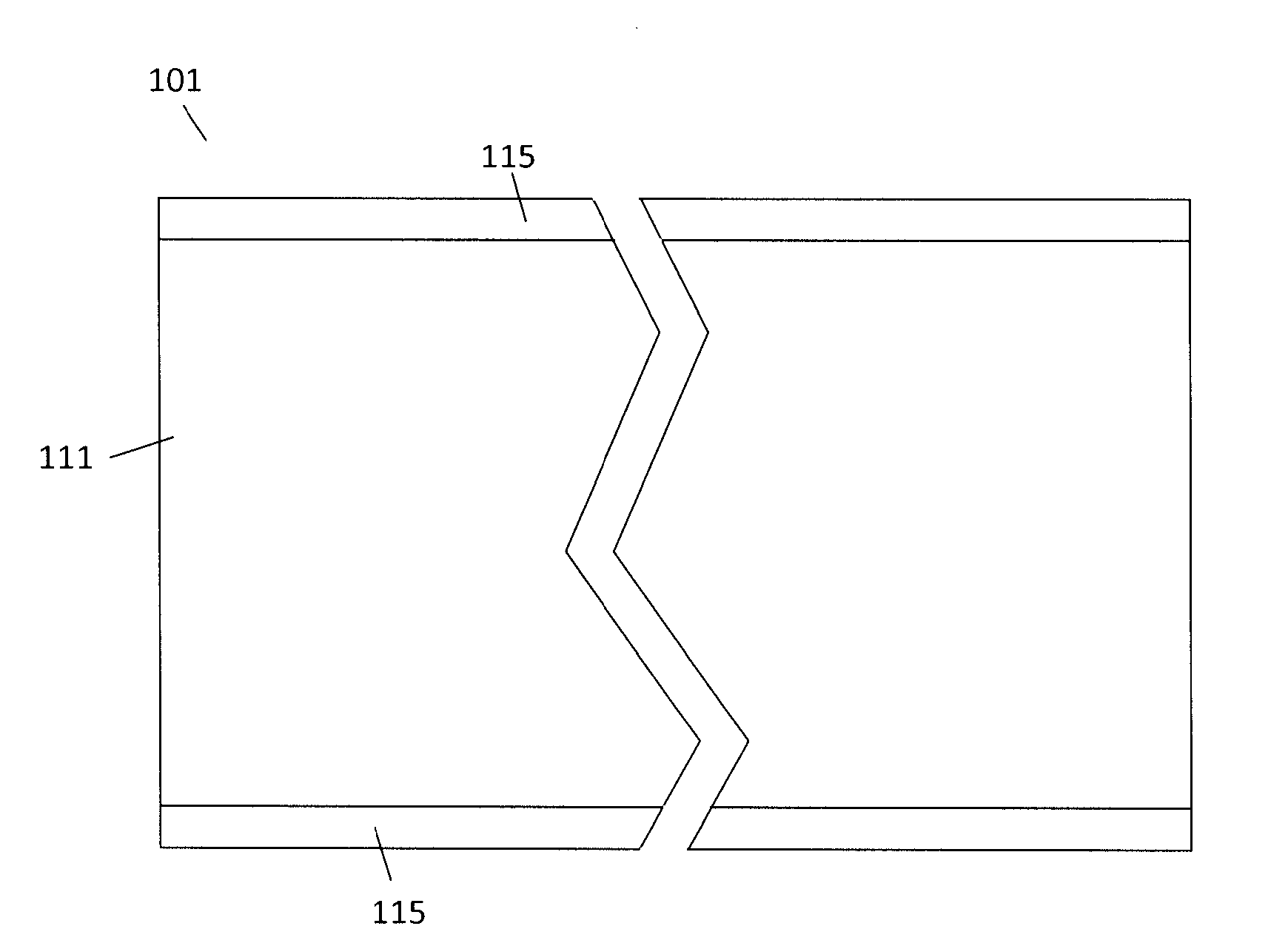
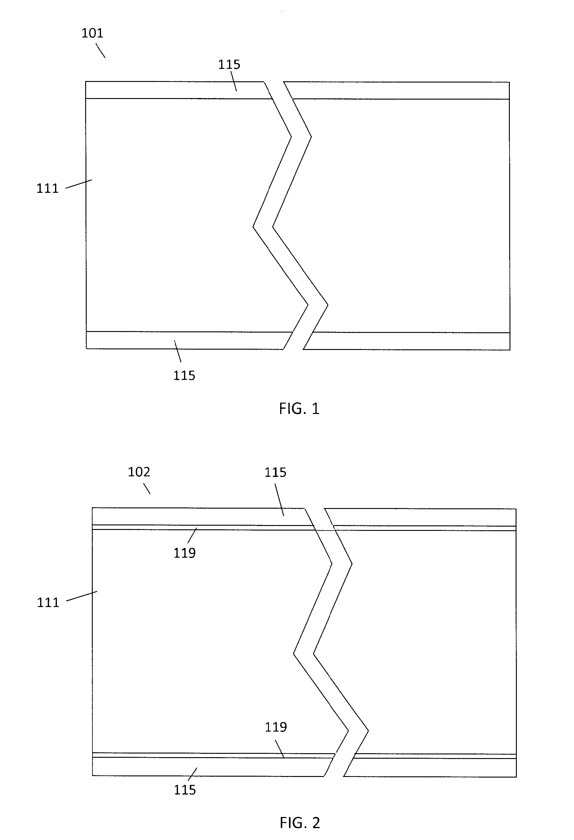
[0020]The present invention is directed towards a polymer based thermally conductive printed circuit board (PCB). With reference to FIG. 1 the PCB 101 includes a polymer substrate 111 and conductive layers 115 bonded to upper and lower surfaces of the polymer substrate 111. The present invention differs from the prior art because the polymer substrate 111 is a dielectric material that also has high thermal conductivity properties that help to dissipate heats from electrical components mounted on the PCB 101. This inherent ability to dissipate heat allows heat producing components to be mounted on the PCB 101 without the addition of a heat sink to keep the component at a thermal equilibrium that is within the acceptable operating temperature range. In this embodiment, the conductive layers 115 are bonded directly to the polymer substrate 111. In another embodiment with reference to FIG. 2, the PCB 102 uses layers of an adhesive bonding agent 119 can be used to bond the conductive lay...


PUM

PropertyMeasurementUnit
Electrical resistanceaaaaaaaaaa
Frequencyaaaaaaaaaa
Electrical resistivityaaaaaaaaaa

Abstract

A printed circuit board has a liquid crystalline polymer layer that is bonded to an electrically conductive layer that includes traces that electrically connect components mounted on the printed circuit board. The liquid crystalline polymer material is thermally conductive and dielectric. When the components produce heat, the liquid crystalline polymer layer absorbs and dissipates the heat produced by the electrical components mounted on the printed circuit board. The thermal equilibrium of the printed circuit board is lower than the maximum operating temperature of the components.

Description

CROSS REFERENCE TO RELATED APPLICATIONS[0001]This US Patent Application claims priority to U.S. Provisional Patent Applications No. 61 / 080,652, “Thermally Conductive Polymer Based Plastic Printed Circuit Board For Single Or Multilayer Applications (TCPPCB)” filed Jul. 14, 2008. U.S. Provisional Patent Application No. 61 / 080,652 is hereby incorporated by reference.FIELD OF INVENTION[0002]The present invention relates to a printed circuit board apparatus and methods for making printed circuit boards.BACKGROUND[0003]Printed circuit boards (PCBs) are used to mechanically support and electrically connect electronic components using conductive pathways, or traces, etched from metal sheets laminated onto a non-conductive substrate. In general, the non-conductive substrates have poor thermal conductivity properties. PCBs can have holes drilled for each wire or electrical connection of each component. The components' leads are passed through the holes and soldered to the traces. This method ...

Claims


Application Information

Patent Timeline
IPC IPC(8): H05K1/00
CPCH05K1/0203H05K1/0313H05K1/0326H05K2201/0145H05K3/388H05K2201/0141H05K3/181
Inventor HEDIN, LOGAN BROOKMILLER, DAVID MICHAEL
Owner HEDIN LOGAN BROOK
Learn More