

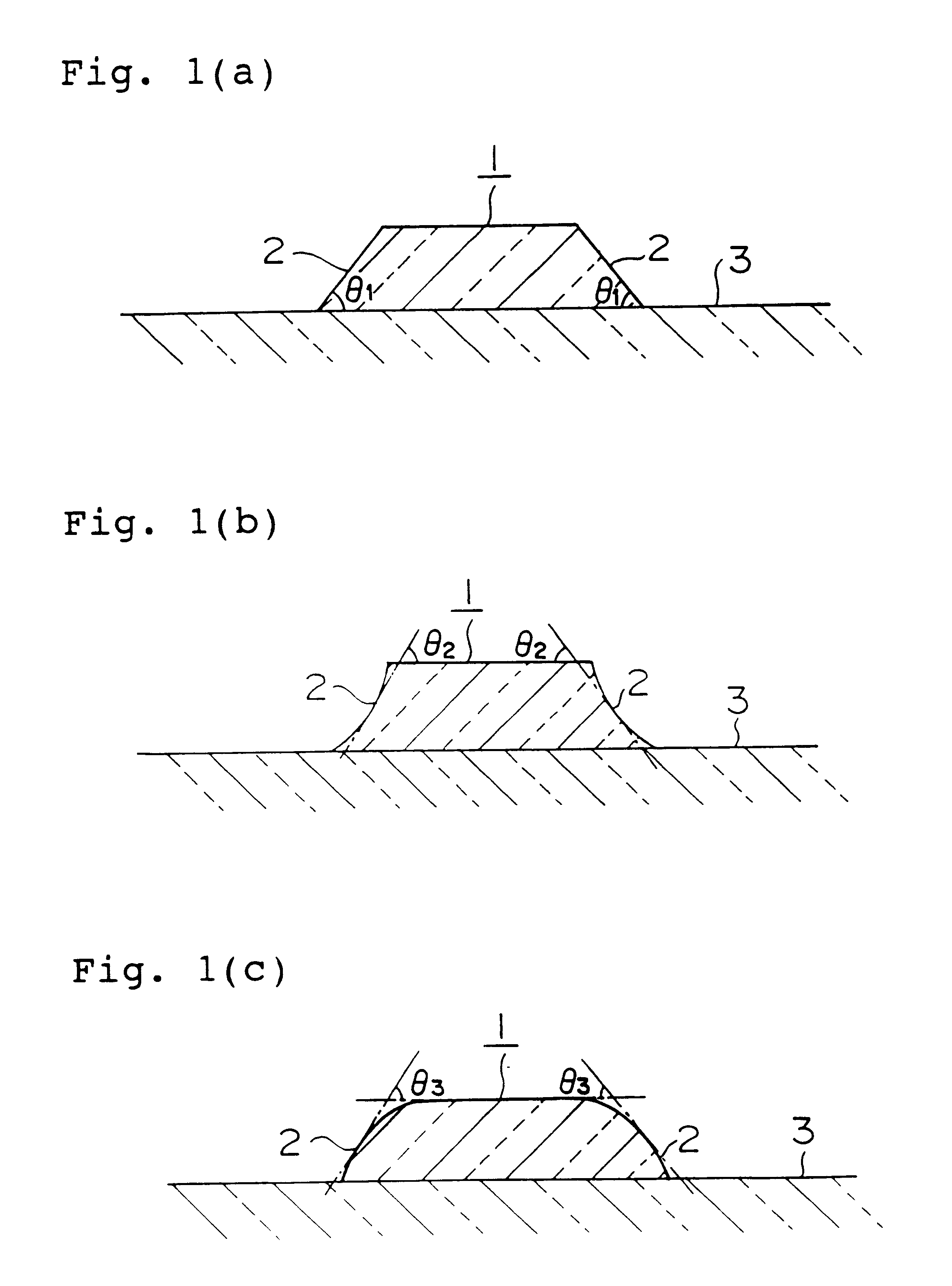
Organic EL device
a technology of organic el and electrodes, which is applied in the direction of discharge tube luminescnet screens, natural mineral layered products, etc., can solve the problems of uneven brightness, impaired flatness of the transparent electrode surface, and accelerated deterioration of the devi
- Summary
- Abstract
- Description
- Claims
- Application Information
AI Technical Summary
Benefits of technology
Problems solved by technology
Method used
Image

Examples
example 1
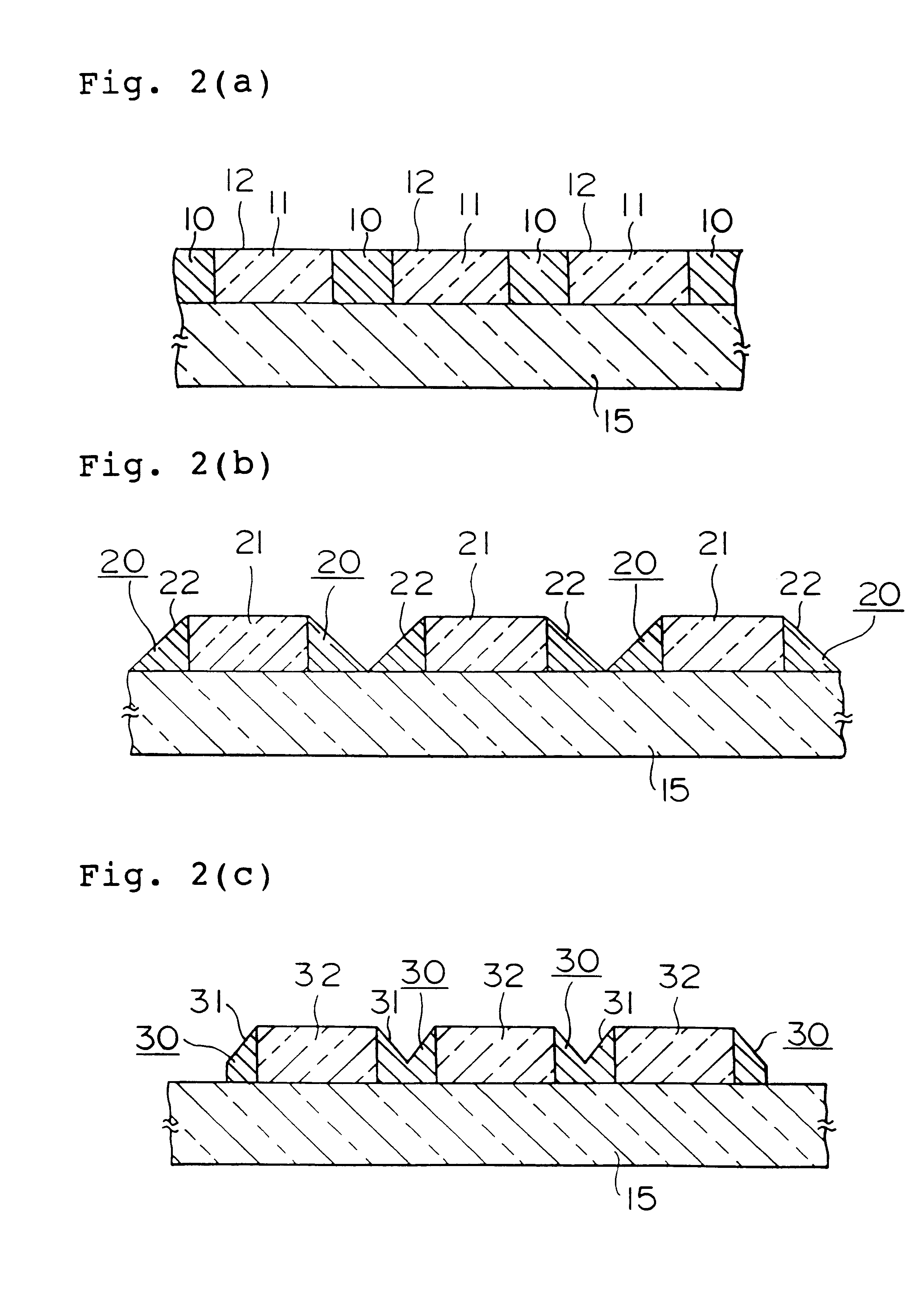
(1) Preparation of transparent electrode
An In--Zn--O-containing amorphous oxide layer (indium atomic ratio, In / (In+Zn),=0.8) having a thickness of 300 nm was formed on one surface of a glass substrate having a size of 75.times.75.times.1.1 mm by a DC magnetron sputtering method using, as a sputtering target, an In--Zn--O-containing oxide sintered body having an indium (In) atomic ratio, In / (In+Zn), of 0.83. The above sputtering was carried out in a sputtering atmosphere containing mixed gases of argon gas and oxygen gas (Ar:O.sub.2 =1,000:2.8 (volume ratio)) at a vacuum degree of 0.2 Pa at a DC sputtering output of 2 W / cm.sup.2. The above amorphous oxide layer was measured for a surface resistance to show 10 .OMEGA. / .quadrature..
Then, the above amorphous oxide layer was processed into two split rows in the form of stripes having a width of 110 .mu.m, a length of 37.5 mm and a pitch of 120 .mu.m by wet-etching using a 12% HBr aqueous solution as an etchant, to obtain a predetermined ...
example 2
An In--Zn--O-containing amorphous oxide layer (atomic ratio of In, In / (In+Zn)=0.8) having a thickness of 300 nm was formed in the same manner as in Example 1(1).
Then, a photoresist film is formed on the above In--Zn--O-containing amorphous oxide layer, and exposure using a predetermined exposure master mask and development using a predetermined developer solution were carried out, to form a resist pattern having a desired form. Then, wet-etching was carried out with a 12% HBr aqueous solution as an etchant. Then, while the above resist pattern was maintained as it was, an aluminum (Al) layer having a thickness of 270 nm was formed on the resist pattern and the glass surface on the side where the resist pattern was formed, by an electron beam deposition method.
Then, the above resist pattern was removed with a predetermined release solution, to give a glass substrate on which two split rows of a predetermined number of In--Zn--O-containing amorphous oxide layer transparent electrode l...
example 3
(1) Preparation of transparent electrode
First, a TiO.sub.2 layer having a thickness of 100 nm was formed on one surface of a glass plate having a size of 75.times.75.times.1.1 mm by an RF magnetron sputtering method, to obtain a transparent substrate having an undercoat layer formed of the above TiO.sub.2 layer. The formation of the TiO.sub.2 layer was carried out under a sputtering atmosphere of argon gas at a sputtering vacuum degree of 0.2 Pa at an RF sputtering output of 2 W / cm.sup.2.
Then, an Ag layer having a thickness of 5 nm was formed on the above TiO.sub.2 layer by a DC magnetron sputtering method. In this case, the sputtering atmosphere and the vacuum degree were the same as those for the formation of the above TiO.sub.2 layer, and the DC sputtering output was set at 1 W / cm.sup.2.
Thereafter, an In--Zn--O-containing amorphous oxide layer (atomic ratio of In, In / (In+Zn)=0.8) having a thickness of 100 nm was formed on the above Ag layer by a DC magnetron sputtering method. In...
PUM
| Property | Measurement | Unit |
|---|---|---|
| Angle | aaaaa | aaaaa |
| Angle | aaaaa | aaaaa |
| Nanoscale particle size | aaaaa | aaaaa |
Abstract
Description
Claims
Application Information