Display device

Active Publication Date: 2014-02-13
SEMICON ENERGY LAB CO LTD
3 Cites 77 Cited by

AI-Extracted Technical Summary

Problems solved by technology

In the case where a display device has a structure in which an electrode of a touch sensor is provided between a pair of substrates included in a display panel, there is a problem in that parasitic capacitance between the electrode of the touch sensor and a wiring and an electrode of the display panel is increased and detection sensitivity of the touch sensor cannot be sufficiently obtained.
Thus, in such a structure, the detection sensitivity of the touch sensor is significantly impaired.
Similarly, in the structure illustrated in FIG. 3B of Patent Documen...

Method used

[0053]Thus, in order to obtain favorable detection sensitivity of a capacitive touch sensor which performs detection using capacitive coupling, it is desirable to achieve at least one of the following: making the parasitic capacitance Cp as small as possible; and making the amount of change in the capacitance for detection as large as possible.
[0056]In the display device 100, the second substrate 102 is positioned closest to the touch surface. Thus, a material and a thickness of the second substrate 102 are preferably determined so that the change in the capacitance (e.g., the above-described mutual capacitance Cf) for detection is made as large as possible. Further, it is preferable that the strength of the second substrate 102 be secured so that damage to the display device 100 due to touch operation is prevented.
[0058]The stress relief layer 104 is formed using a material whose product of the specific gravity and dielectric constant is smaller than that of the second substrate 102, whereby parasitic capacitance generated between the electrode of the sensor layer 103 and the electrode of the display element layer 106 can be effectively reduced while the increase in the weight due to the provision of the stress relief layer 104 is suppressed. Further, the second substrate 102 is formed using a material whose product of the specific gravity and dielectric constant is larger than that of the stress relief layer 104, so that the change in the capacitance for detection can be increased without damaging the strength. Thus, the decrease in the parasitic capacitance and the increase in the capacitance for detection enable the detection sensitivity of the touch sensor to be extremely high.
[0063]Here, the liquid crystal element preferably has an IPS mode or an FFS mode. A liquid crystal element having such a mode does not require an electrode to be provided on the second substrate 102 side. Thus, it is possible to reduce the influence of parasitic capacitance generated between an electrode of the touch sensor provided on the second substrate 102 side and the electrode of the liquid crystal element, thereby improving the sensitivity of the touch sensor.
[0065]In order to protect the surface of the polarizing plate 122, the protective substrate 124 is provided over a surface of the polarizing plate 122 which is opposite to the surface facing the second substrate 102. Here, mechanical strength of the protective substrate 124 is preferably high because one surface of the protective substrate 124 serves as a touch surface.
[0067]The display device 120 includes the stress relief layer 104 between the sensor layer 103 and the color filter layer 105 and thus is lightweight and has high sensitivity of the touch sensor.
[0070]The stress relief layer 114 having such a function is provided between the sensor layer 103 and the color filter layer 105, whereby it is not necessary to provide the polarizing plate 122 and the protective substrate 124 outside the second substrate 102. Thus, the weight of the display device 130 can be further reduced. Further, a surface of second substrate 102, which does not face the sensor layer 103, acts as a touch surface by omission of the polarizing plate 122 and the protective substrate 124. Therefore, the change in capacitance for detection between the touch surface and the sensor layer 103 can be increased and detection sensitivity can be extremely high.
[0075]In any of the display devices described in this embodiment, the sensor is provided between the first substrate and the second substrate and the stress relief layer is provided between the sensor layer and the color filter layer. Further, the product of the specific gravity and dielectric constant of the stress relief layer is smaller than that of the second substrate. Thus, a display device that is extremely lightweight and has high sensitivity of the touch sensor can be realized.
[0085]The thickness of the second substrate 102 is determined depending on the material. For example, in the case of using a glass material, the thickness is preferably set to greater than or equal to 10 μm and less than or equal to 2 mm, preferably greater than or equal to 50 μm and less than or equal to 1 mm. As the second substrate 102 is thinner, the detection sensitivity of the touch sensor can be improved.
[0101]Subsequently, a planarization layer 155 is formed over the stress relief layer 154. The planarization layer 155 can be formed using a material similar to that used for the insulating layer 151. The planarization layer 155 is provided so as to planarize the surface of the stress relief layer 154 by covering the surface thereof. The provision of the planarization layer 155 makes it possible to suppress variation in the thickness of the color filters in the color filter layer 105 to be formed later and variation in luminance among pixels. Further, the provision of the planarization layer 155 makes it possible to protect the surface of the stress relief layer 154 in a later formation process of the color filter layer 105. Note that in the case where the top surface of the stress relief layer 154 is sufficiently planarized and is able to withstand the formation of the color filter layer 105, the planarization layer 155 is not necessarily provided.
[0109]Through the above steps, the display device 150 can be manufactured. In the display device 150, layers of the stress relief layer 154, the insulating layer 151, the bonding layer 153, the planarization layer 155, the color filter layer 105, and the like are provided between the electrode of the liquid crystal element layer 121 and the electrode (the electrode 111 or the electrode 112) of the sensor layer 103 for detection; thus, parasitic capacitance generated between the electrodes is extremely reduced. Further, the stress relief layer 154 contains a polarizer and functions as a polarizing plate; thus, one surface of the second substrate 102 can be used as a touch surface. With such a structure, a display device that is lightweight and whose touch sensor has high sensitivity can be realized.
[0123]Then, by applying physical force gradually from the starting point of separation in a direction substantially perpendicular to the attachment surfaces, separation can be easily caused without damage to the support substrate 161. At this time, for example, separation may be caused by attaching tape or the like to the support substrate 161 and pulling the tape in the aforementioned direction, or separation may be caused by pulling an end portion of the support substrate 161 with a hook-like member. Alternatively, separation may be caused by attaching a member capable of vacuum suction to the back side of the support substrate 161.
[0138]Here, the electrode 112 is in the form of a series of quadrangles arranged in one direction as illustrated in FIGS. 7A and 7B. The electrode 111 is also in the form of a quadrangle. A plurality of electrodes 111 arranged in a line in a direction intersecting the direction in which the electrode 112 extends is electrically connected to each other by the wiring 152. The electrode 112 and the wiring 152 are preferably arranged so that the area of the intersecting portion of the electrode 112 and the wiring 152 becomes as small as possible. Such a shape can reduce the area of a region where the electrodes are not provided and decrease luminance unevenness of light passing through the touch sensor 202 which may be caused by a difference in transmittance depending on whether the electrodes are provided or not.
[0145]Further, there is no particular limitation on the crystallinity of a semiconductor used for the transistors, and an amorphous semiconductor or a semiconductor having crystallinity (a microcrystalline semiconductor, a polycrystalline semiconductor, or a semiconductor partly including crystal regions) may be used. A semiconductor having crystallinity is preferably used, in which case deterioration of transistor characteristics can be reduced.
[0146]Typical examples of the oxide semiconductor containing at least one of indium, gallium, and zinc include an In—Ga—Zn-based metal oxide, and the like. An oxide semiconductor having a wider band gap and a lower carrier density than silicon is preferably used because off-state leakage current can be reduced. Details of preferred oxide semiconductors will be described below in another embodiment.
[0151]The color filter 243 is provided in order to adjust the color of light transmitted through a pixel to increase the color purity. For example, in a full-color display device using a white back light, a plurality of pixels provided with color filters of different colors are used. In that case, the color filters may be those of three colors of R (red), G (green), and B (blue) or four colors (yellow (Y) in addition to these three colors). Further, a white (W) pixel may be added to R, G, and B (and Y), i.e., color filters of four colors (or five colors) may be used.
[0152]A black matrix 242 is provided between the adjacent color filters 243. The black matrix 242 blocks light emitted from an adjacent pixel, thereby preventing color mixture between the adjacent pixels. In one configuration, the black matrix 242 may be provided only between adjacent pixels of different emission colors and not between pixels of the same emission color. Here, the color filter 243 is provided so that its end portions overlap with the black matrix 242, whereby light leakage can be reduced. The black matrix 242 can be formed using a material that blocks light transmitted through the pixel, for exampl...

Benefits of technology

[0025]According to the present invention, in a display device provided with a touch sensor, a reduction in...

Abstract

A reduction in the weight of a display device with a touch sensor is achieved while a decrease in the sensitivity thereof is suppressed. The display device includes, between a pair of substrates, a touch sensor, a color filter, and a display portion provided with a display element. A stress relief layer whose product of the dielectric constant and specific gravity is smaller than that of the substrate provided with the touch sensor is provided, whereby parasitic capacitance between an electrode and a wiring included in the touch sensor and an electrode and a wiring included in the display portion can be reduced.

Application Domain

Technology Topic

Image

  • Display device
  • Display device
  • Display device

Examples

  • Experimental program(9)

Example

Embodiment 1
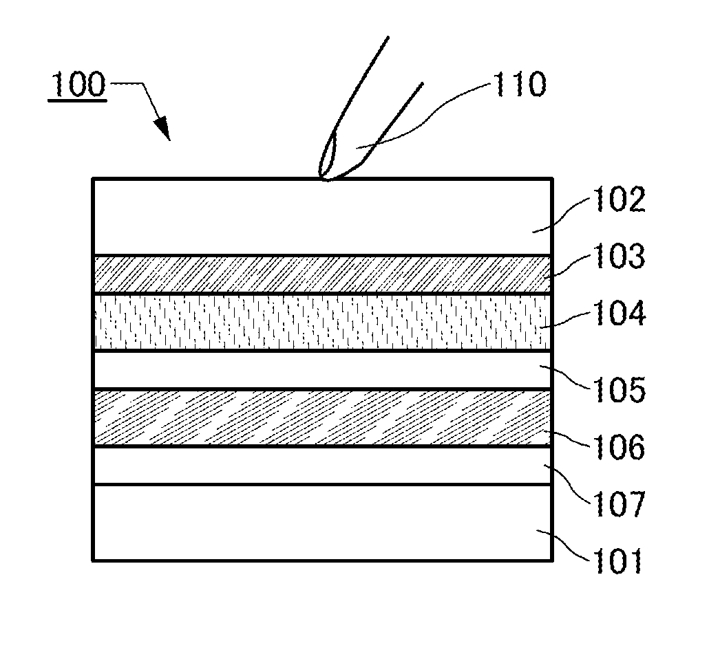
[0040]In this embodiment, a structural example of a display device according to one embodiment of the present invention is described with reference to drawings.
[0041]FIG. 1 is a schematic view of a display device 100 exemplified in this embodiment. The display device 100 includes a first substrate 101 and a second substrate 102. Between the first substrate 101 and the second substrate 102, a TFT layer 107, a display element layer 106, a color filter layer 105, a stress relief layer 104, and a sensor layer 103 are stacked in this order from the first substrate 101 side.
[0042]The TFT layer 107 includes a transistor, a wiring, and the like for driving the display element layer 106. Note that in the case of a passive matrix display device, a transistor is not necessary, and only a wiring and an electrode are provided.
[0043]The display element layer 106 includes a plurality of display elements. Each of the display elements includes at least a pair of electrodes. As the display element, typically, a liquid crystal element, an organic EL element, or the like can be used. In addition, a display element in which an electrophoresis element or the like is interposed between the pair of electrodes may be used.
[0044]The color filter layer 105 includes color filters overlapping with the display elements in the display element layer 106. For example, when the color filter layer 105 is provided with three color filters of red (R), green (G), and blue (B), a display device capable of full-color display can be obtained. The color filter layer 105 may include a black matrix or the like in addition to the color filters.
[0045]The sensor layer 103 functions as a touch sensor which senses proximity or touch of a conductive object to be sensed such as a finger 110 to the second substrate 102 from the outside. As the touch sensor provided for the sensor layer 103, a capacitive touch sensor is preferable. Examples of the capacitive touch sensor are of a surface capacitive type, of a projected capacitive type, and the like. Further, examples of the projected capacitive type are of a self capacitive type, a mutual capacitive type, and the like mainly in accordance with the difference in the driving method. The use of a mutual capacitive type is preferable because multiple points can be sensed simultaneously.
[0046]Here, the operation of a capacitive touch sensor and the influence of parasitic capacitance on detection sensitivity are described. FIG. 2A is a schematic view of a mutual capacitive touch sensor. For simplicity, an example of one sensor element is described here.
[0047]The sensor element includes a pair of electrodes (an electrode 111 and an electrode 112). Mutual capacitance Cf is formed between the electrode 111 and the electrode 112. Further, each of the electrode 111 and the electrode 112 is connected to a parasitic capacitance Cp.
[0048]AC voltage (or pulse voltage) is input to the electrode 111. Further, a sensor unit which senses current is electrically connected to the electrode 112. Thus, in accordance with a change in voltage input to the electrode 111, current Is flowing through the electrode 112 coupled to the electrode 111 by the mutual capacitance Cf can be sensed by the sensor unit. Here, the value of current Is is proportional to the value of the mutual capacitance Cf.
[0049]Here, as illustrated in FIG. 2B, when a conductive object to be sensed such as a finger or the like comes close to the pair of electrodes of the sensor element, the value of the mutual capacitance Cf is reduced. Thus, in accordance with the change in the mutual capacitance Cf, the value of current Is flowing through the electrode 112 is reduced. By detecting the difference in the current Is, touch operation can be detected.
[0050]However, when the value of parasitic capacitance Cp connected to the electrode 111 and the electrode 112 is large, the value of current flowing through the electrode 112 is reduced by capacitive coupling. As a result, detection sensitivity of the touch operation is reduced.
[0051]As another example, FIG. 2C is a schematic view of a self capacitive touch sensor. In the self capacitive touch sensor, constant potential is applied to the electrode 111, and current Is at the time when AC voltage is applied to the electrode 112 that is capacitively coupled to the electrode 111 by self-capacitance Cs is sensed. The self-capacitance Cs is changed by the presence or absence of an object to be sensed. By detecting the change in the current Is owing to the change in the self-capacitance Cs, touch operation can be detected. However, similarly to the above, the larger the parasitic capacitance Cp connected to the electrode 112 is, the smaller the change in the current Is is; thus, detection sensitivity is decreased.
[0052]Note that such a problem of a decrease in the detection sensitivity due to the parasitic capacitance Cp occurs in a general capacitive touch sensor which performs detection using capacitive coupling, such as a surface capacitive touch sensor.
[0053]Thus, in order to obtain favorable detection sensitivity of a capacitive touch sensor which performs detection using capacitive coupling, it is desirable to achieve at least one of the following: making the parasitic capacitance Cp as small as possible; and making the amount of change in the capacitance for detection as large as possible.
[0054]The above is the description of the touch sensor.
[0055]The display device 100 illustrated in FIG. 1 includes the stress relief layer 104 between the sensor layer 103 and the color filter layer 105. The product of the specific gravity and dielectric constant of the stress relief layer 104 is smaller than that of the second substrate 102.
[0056]In the display device 100, the second substrate 102 is positioned closest to the touch surface. Thus, a material and a thickness of the second substrate 102 are preferably determined so that the change in the capacitance (e.g., the above-described mutual capacitance Cf) for detection is made as large as possible. Further, it is preferable that the strength of the second substrate 102 be secured so that damage to the display device 100 due to touch operation is prevented.
[0057]The change in the capacitance for detection is increased by thinning the second substrate 102; however, the strength of the second substrate 102 is decreased. Thus, as a material for the second substrate 102, a material having a high dielectric constant is preferably used for securing the strength. The use of an insulating material with a large specific gravity is preferable because the strength and the dielectric constant can be increased.
[0058]The stress relief layer 104 is formed using a material whose product of the specific gravity and dielectric constant is smaller than that of the second substrate 102, whereby parasitic capacitance generated between the electrode of the sensor layer 103 and the electrode of the display element layer 106 can be effectively reduced while the increase in the weight due to the provision of the stress relief layer 104 is suppressed. Further, the second substrate 102 is formed using a material whose product of the specific gravity and dielectric constant is larger than that of the stress relief layer 104, so that the change in the capacitance for detection can be increased without damaging the strength. Thus, the decrease in the parasitic capacitance and the increase in the capacitance for detection enable the detection sensitivity of the touch sensor to be extremely high.

Example

APPLICATION EXAMPLE
[0059]An example where a liquid crystal element is applied to the display element included in the display element layer 106 and an example where a light-emitting element is applied to the display element included in the display element layer 106 are described below.
[0060]A display device 120 illustrated in FIG. 3A is different from the display device 100 illustrated in FIG. 1 in that a liquid crystal element layer 121 is used instead of the display element layer 106 and a polarizing plate 122, a polarizing plate 123, and a protective substrate 124 are used.
[0061]The liquid crystal element layer 121 includes a liquid crystal element provided with a pair of electrodes and a liquid crystal. As the liquid crystal, a thermotropic liquid crystal, a low molecular liquid crystal, a high molecular liquid crystal, a ferroelectric liquid crystal, an anti-ferroelectric liquid crystal, or the like can be used. Moreover, a liquid crystal exhibiting a blue phase is preferably used because an alignment film is not necessary and the viewing angle is wide.
[0062]As a structure of the liquid crystal element, any of the following can be used: an in-plane-switching (IPS) mode, a twisted nematic (TN) mode, a vertical alignment (VA) mode, a fringe field switching (FFS) mode, an axially symmetric aligned micro-cell (ASM) mode, an optically compensated birefringence (OCB) mode, a ferroelectric liquid crystal (FLC) mode, an antiferroelectric liquid crystal (AFLC) mode, and the like.
[0063]Here, the liquid crystal element preferably has an IPS mode or an FFS mode. A liquid crystal element having such a mode does not require an electrode to be provided on the second substrate 102 side. Thus, it is possible to reduce the influence of parasitic capacitance generated between an electrode of the touch sensor provided on the second substrate 102 side and the electrode of the liquid crystal element, thereby improving the sensitivity of the touch sensor.
[0064]The polarizing plate 122 is provided over a surface of the second substrate 102 which is opposite to the surface facing the sensor layer 103. The polarizing plate 123 is provided on a surface of the first substrate 101 which is opposite to the surface facing the TFT layer 107.
[0065]In order to protect the surface of the polarizing plate 122, the protective substrate 124 is provided over a surface of the polarizing plate 122 which is opposite to the surface facing the second substrate 102. Here, mechanical strength of the protective substrate 124 is preferably high because one surface of the protective substrate 124 serves as a touch surface.
[0066]By controlling transmission of light from a backlight 115 provided on the first substrate 101 side of the display device 120, display of the display device 120 can be performed.
[0067]The display device 120 includes the stress relief layer 104 between the sensor layer 103 and the color filter layer 105 and thus is lightweight and has high sensitivity of the touch sensor.
[0068]FIG. 3B illustrates a structural example of a display device 130 whose structure is partly different from that of the display device 120. The display device 130 is different from the display device 120 in that a stress relief layer 114 is provided instead of the stress relief layer 104 and that the polarizing plate 122 and the protective substrate 124 are not provided.
[0069]The stress relief layer 114 includes a polarizer and functions as a polarizing plate which polarizes light from the backlight 115 which has passed through the liquid crystal element in the liquid crystal layer 121.
[0070]The stress relief layer 114 having such a function is provided between the sensor layer 103 and the color filter layer 105, whereby it is not necessary to provide the polarizing plate 122 and the protective substrate 124 outside the second substrate 102. Thus, the weight of the display device 130 can be further reduced. Further, a surface of second substrate 102, which does not face the sensor layer 103, acts as a touch surface by omission of the polarizing plate 122 and the protective substrate 124. Therefore, the change in capacitance for detection between the touch surface and the sensor layer 103 can be increased and detection sensitivity can be extremely high.
[0071]A display device 140 illustrated in FIG. 4 is different from the display device 100 illustrated in FIG. 1 in that a light-emitting element layer 131 is used instead of the display element layer 106.
[0072]The light-emitting element layer 131 includes a light-emitting element in which a layer containing a light-emitting organic compound is provided between a pair of electrodes. A specific structural example of the light-emitting element will be described in an embodiment below.
[0073]The display device 140 having such a structure needs neither a back light nor a polarizing plate and thus can be lighter than the display device in which a liquid crystal element is used.
[0074]The above is the description of the application examples.
[0075]In any of the display devices described in this embodiment, the sensor is provided between the first substrate and the second substrate and the stress relief layer is provided between the sensor layer and the color filter layer. Further, the product of the specific gravity and dielectric constant of the stress relief layer is smaller than that of the second substrate. Thus, a display device that is extremely lightweight and has high sensitivity of the touch sensor can be realized.
[0076]This embodiment can be implemented in an appropriate combination with any of the other embodiments described in this specification.

Example

Embodiment 2
[0077]In this embodiment, as an example of a method for manufacturing a display device of one embodiment of the present invention, an example of a method for manufacturing a display device in which a liquid crystal element is used is described with reference to drawings.
Example of Manufacturing Method 1
[0078]First, a TFT layer 107 is formed over the first substrate 101 (see FIG. 5A).
[0079]The first substrate 101 is formed using a material having an insulating surface and having light-transmitting properties to visible light. A glass material, a resin material, or the like can be used for the material of the first substrate 101. Further, when the display device is used with being curved, a flexible resin material, a glass material that is thin enough to have flexibility, or a composite material or a laminated material of these materials is used for the first substrate 101.
[0080]The TFT layer 107 includes at least a transistor. The TFT layer 107 may include a capacitor in addition to the transistor. Further, the TFT layer 107 may include a driving circuit (a gate driving circuit, a source driving circuit), and the like. Furthermore, the TFT layer 107 may include a wiring and an electrode.
[0081]The TFT layer 107 can be manufactured by an appropriate manufacturing method. For example, in the case of an active matrix display device in which a liquid crystal element is used, a gate electrode (and a wiring), a gate insulating layer, a semiconductor layer, and a source electrode and a drain electrode (and wirings) which form a transistor are provided over the first substrate 101. Further, an electrode of the liquid crystal element is formed thereover so as to be electrically connected to the transistor. Note that the electrode becomes part of the liquid crystal element layer 121 to be formed later. Further, an alignment film for controlling alignment of a liquid crystal may be formed over the electrode.
[0082]Subsequently, the sensor layer 103 is formed over the second substrate 102 (FIG. 5B). Here, the case of using a projected capacitive touch sensor for the sensor layer 103 is described.
[0083]First, the second substrate 102 is prepared. For the second substrate 102, a material similar to that used for the first substrate 101 can be used. Note that in the case where a surface of the second substrate 102 on which the sensor layer 103 is not formed is a touch surface, a glass substrate, specifically, a tempered glass substrate with increased strength is preferably used as the second substrate 102. Alternatively, a resin material whose surface is coated with a hard layer formed using an inorganic material may be used. Further, when the display device is used with being curved, a flexible resin material, a glass material that is thin enough to have flexibility, or a composite material or a laminated material of these materials is used for the second substrate 102.
[0084]For example, as an example of a glass material that can be used for the second substrate 102, a glass material whose dielectric constant is greater than or equal to 3.5 and less than or equal to 10.0, and specific gravity is greater than or equal to 2.0 and less than or equal to 4.5 can be given.
[0085]The thickness of the second substrate 102 is determined depending on the material. For example, in the case of using a glass material, the thickness is preferably set to greater than or equal to 10 μm and less than or equal to 2 mm, preferably greater than or equal to 50 μm and less than or equal to 1 mm. As the second substrate 102 is thinner, the detection sensitivity of the touch sensor can be improved.
[0086]Next, the electrode 111 and the electrode 112 which have light-transmitting properties are formed over the second substrate 102. The electrode 111 and the electrode 112 are formed in such a manner that after a conductive film is formed by a sputtering method or the like, an unnecessary portion of the conductive film is removed using a patterning technique such as a photolithography method.
[0087]Next, an insulating layer 151 having light-transmitting properties, which covers the electrode 111 and the electrode 112, is formed. The insulating layer 151 is preferably formed using a material whose product of the specific gravity and dielectric constant is smaller than that of the second substrate 102. As a material of the insulating layer 151, for example, a resin such as acrylic or epoxy, a resin having a siloxane bond, or an inorganic insulating material such as silicon oxide, silicon oxynitride, or an aluminum oxide an be used.
[0088]Next, after openings which reach the electrode 111 are formed in the insulating layer 151, a wiring 152 that is electrically connected to the electrode 111 is formed over the insulating layer 151. The wiring 152 is preferably formed using a material that has higher conductivity than each of the electrode 111 and the electrode 112.
[0089]The electrode 112 is provided in the form of stripes in one direction (a direction perpendicular to the paper). Further, the electrode 111 is provided such that the electrode 112 is sandwiched by a pair of electrodes 111, and the wiring 152 that electrically connects the pair of electrodes 111 is provided so as to intersect with the electrode 112. Here, one electrode 112 and a plurality of electrodes 111 electrically connected to each other by the wiring 152 do not necessarily intersect orthogonally and may form an angle of less than 90°.
[0090]Through the above steps, the sensor layer 103 can be formed over the second substrate 102.
[0091]Subsequently, the stress relief layer 154 is formed over the sensor layer 103 (FIG. 5C).
[0092]The stress relief layer 154 can have the same structure as those of the stress relief layer 104 and the stress relief layer 114 that are described in Embodiment 1.
[0093]As the stress relief layer 154, for example, a resin such as acrylic, epoxy, polyimide, polyamide, polyamideimide, polyethylene terephthalate (PET), polyethylene naphthalate (PEN), polybutylene terephthalate (PBT), polyarylalte (PAR), polyether sulfone (PES), polycarbonate (PC), polyether etherketone (PEEK), polysulfone (PSF), polyether imide (PEI), acrylonitrile-butadiene styrene, polyvinyl chloride, polypropylene, polyvinyl acetate, polyester, or a resin having a siloxane bond, or a glass such as barium borosilicate glass, or aluminoborosilicate glass, or the like can be used.
[0094]Further, a resin containing a polarizer is preferably used as the stress relief layer 154 so as to have a function as a polarizing plate. In that case, a material capable of producing linearly polarized light from natural light or circularly polarized light is used. For example, a material whose optical anisotropy is obtained by disposing dichroic substances in one direction can be used. For example, the stress relief layer 154 can be formed in such a manner that an iodine-based compound or the like is adsorbed to a film or the like such as a polyvinyl alcohol film and the film or the like is stretched in one direction. Note that as the dichroic substance, a dye-based compound or the like as well as an iodine-based compound can be used.
[0095]The stress relief layer 154 is formed using a material having a film shape, a sheet shape, or a plate shape.
[0096]The stress relief layer 154 having a film shape can be formed by spin coating, dip coating, spray coating, a droplet discharge method, a printing method such as a screen printing method, or a formation method using a tool such as a doctor knife, a roll coater, a curtain coater, or a knife coater.
[0097]In the case of using the material having a film shape, a sheet shape or a plate shape, the material is attached to the sensor layer 103 with the a bonding layer 153 provided therebetween. The bonding layer 153 is acceptable as long as it has light-transmitting properties and can bond the stress relief layer 154 and a surface to be bonded. The bonding layer 153 can be formed using a thermosetting resin or an ultraviolet curable resin. For example, an acrylic resin, a urethane resin, an epoxy resin, or a resin having a siloxane bond can be used.
[0098]For example, in the case of using an acrylic resin as the stress relief layer 154, acrylic whose dielectric constant is greater than or equal to 2.5 and less than or equal to 4.5 and specific gravity is greater than or equal to 1.0 and less than or equal to 1.3 is used. The use of a material containing a resin as the stress relief layer 154 is preferable because both dielectric constant and specific gravity can be reduced.
[0099]The thickness of the stress relief layer 154 can be set depending on the material. In the case of using an acrylic resin, the thickness thereof is set to greater than or equal to 5 μm and less than or equal to 3 mm, preferably greater than or equal to 10 μm and less than or equal to 2 mm.
[0100]In this embodiment, a material containing a polarizer and having a sheet shape is used for the stress relief layer 154, and the stress relief layer 154 is attached to the sensor layer 103 with the use of the bonding layer 153.
[0101]Subsequently, a planarization layer 155 is formed over the stress relief layer 154. The planarization layer 155 can be formed using a material similar to that used for the insulating layer 151. The planarization layer 155 is provided so as to planarize the surface of the stress relief layer 154 by covering the surface thereof. The provision of the planarization layer 155 makes it possible to suppress variation in the thickness of the color filters in the color filter layer 105 to be formed later and variation in luminance among pixels. Further, the provision of the planarization layer 155 makes it possible to protect the surface of the stress relief layer 154 in a later formation process of the color filter layer 105. Note that in the case where the top surface of the stress relief layer 154 is sufficiently planarized and is able to withstand the formation of the color filter layer 105, the planarization layer 155 is not necessarily provided.
[0102]Next, the color filter layer 105 is formed over the planarization layer 155 (FIG. 5D). The color filter layer 105 can be formed using a photosensitive material including a pigment by a photolithography method. Further, as the color filter layer 105, a black matrix may be provided between color filters with different colors. Further, an overcoat is preferably provided so as to cover the color filters and the black matrix.
[0103]Note that one of electrodes of the liquid crystal element may be formed on the color filter layer 105 in accordance with the structure of the liquid crystal element. Note that the electrode becomes part of the liquid crystal element layer 121 to be formed later. Further, an alignment film may be formed over the electrode.
[0104]Through the above steps, the sensor layer 103, the stress relief layer 154, and the color filter layer 105 can be stacked over the second substrate 102.
[0105]Note that there is no limitation on the order of the step of forming the TFT layer 107 over the first substrate 101 and the step of forming the sensor layer 103, the stress relief layer 154, and the color filter layer 105 over the second substrate 102. Either of the steps may be conducted first, or the two steps may be concurrently conducted.
[0106]Next, a liquid crystal is sealed by a sealant 156 in a state of being interposed between the first substrate 101 and the second substrate 102, whereby the liquid crystal element layer 121 is formed (FIG. 5E).
[0107]The liquid crystal can be formed by a dispenser method (a dropping method), or an injecting method by which a liquid crystal is injected using a capillary phenomenon after the first substrate 101 is attached to the second substrate 102.
[0108]As the sealant 156, a material similar to that used for the bonding layer 153 can be used. Further, the sealant 156 may be formed using glass frit including low-melting glass.
[0109]Through the above steps, the display device 150 can be manufactured. In the display device 150, layers of the stress relief layer 154, the insulating layer 151, the bonding layer 153, the planarization layer 155, the color filter layer 105, and the like are provided between the electrode of the liquid crystal element layer 121 and the electrode (the electrode 111 or the electrode 112) of the sensor layer 103 for detection; thus, parasitic capacitance generated between the electrodes is extremely reduced. Further, the stress relief layer 154 contains a polarizer and functions as a polarizing plate; thus, one surface of the second substrate 102 can be used as a touch surface. With such a structure, a display device that is lightweight and whose touch sensor has high sensitivity can be realized.
[0110]The above is the description of Example of Manufacturing Method 1.
Example of Manufacturing Method 2
[0111]An example of a method for manufacturing a display device, which is partly different from the above-described Example of Manufacturing Method 1, is described with reference to drawings below. Note that description of the same portions as those in Example of Manufacturing Method 1 is skipped or simplified in some cases.
[0112]First, as in Example of Manufacturing Method 1, the TFT layer 107 is formed over the first substrate 101.
[0113]Similarly to the above description, the sensor layer 103 and the stress relief layer 154 are formed over the second substrate 102.
[0114]Here, a support substrate 161 is prepared. A substrate having a relatively planarized surface is used as the support substrate 161. As the support substrate 161, a non-light-transmitting substrate such as a metal substrate or a ceramic substrate can be used other than a substrate using a material similar to that used for the first substrate 101 or the second substrate 102.
[0115]Subsequently, a separation layer 162 and a layer to be separated 163 are stacked over the support substrate 161. Here, a combination of materials which can be separated at the interface of the separation layer 162 and the layer to be separated 163 is used for the separation layer 162 and the layer to be separated 163.
[0116]For example, a metal such as tungsten is used for the separation layer 162, and an oxide such as silicon oxide is used for the layer to be separated 163. At this time, a surface of the metal is oxidized by contact with the oxide, and an oxide of the metal (e.g., tungsten oxide) is formed. Here, the interface between the separation layer 162 and the layer to be separated 163 is physically separated by application of external force.
[0117]Alternatively, a metal and a resin may be used as the separation layer 162 and the layer to be separated 163, respectively; in such a case, separation can be performed by the control of adhesion between the separation layer 162 and the layer to be separated 163. Further alternatively, the separation layer 162 and the layer to be separated 163 each may have a surface with high planarity; in such a case, bonding can be performed by close contact between the two surfaces with high planarity.
[0118]Note that a surface of the support layer 161 may be used as the separation layer 162 and the layer to be separated 163 may be formed on and in contact with the support substrate 161. For example, a metal substrate and a resin can be used as the support substrate 161 and the layer to be separated 163, respectively. Alternatively, for example, a relatively thick glass substrate and a relatively thin glass substrate can be used as the support substrate 161 and the layer to be separated 163, respectively; in such a case, bonding can be performed by close contact between the two surfaces with high planarity.
[0119]Next, the color filter layer 105 is formed on the layer to be separated 163 (FIG. 6A). The color filter layer 105 can be formed by a method similar to the method described in Example of Manufacturing Method 1.
[0120]Next, the second substrate 102 and the support substrate 161 are attached to each other with a bonding layer 164 so that the sensor layer 103 and the color filter layer 105 face each other. Here, for the bonding layer 164, a material similar to that used for the bonding layer 153 can be used.
[0121]After the second substrate 102 and the support substrate 161 are attached to each other, separation is caused at the interface between the separation layer 162 and the layer to be separated 163, so that the support substrate 161 is separated (FIG. 6B).
[0122]As the method for separation, for example, the second substrate 102 is fixed by a suction stage or the like and a starting point of separation is formed between the separation layer 162 and the layer to be separated 163. For example, the starting point of separation may be formed by inserting a sharp instrument such as a knife into the boundary. Alternatively, the starting point of separation may be formed by dripping a liquid that has low surface tension (such as alcohol or water) onto end portions of the two substrates so that the liquid penetrates into the boundary between the two substrates.
[0123]Then, by applying physical force gradually from the starting point of separation in a direction substantially perpendicular to the attachment surfaces, separation can be easily caused without damage to the support substrate 161. At this time, for example, separation may be caused by attaching tape or the like to the support substrate 161 and pulling the tape in the aforementioned direction, or separation may be caused by pulling an end portion of the support substrate 161 with a hook-like member. Alternatively, separation may be caused by attaching a member capable of vacuum suction to the back side of the support substrate 161.
[0124]At the time of separation, static electricity might be generated and the second substrate 102 might be charged therewith. When the second substrate 102 is charged, a circuit or an element in the sensor layer 103 might be damaged by electrostatic discharge (ESD). In order to suppress this, separation is preferably caused in a state where a conductive liquid (e.g., an ionic liquid, water including ions such as carbonated water, or the like) is dripped onto the starting point of separation and the liquid is constantly in contact with the separation interface. Alternatively, separation may be caused while the generation of ESD is being suppressed using an ionizer or the like.
[0125]Next, a liquid crystal is provided between the first substrate 101 and the second substrate 102 and is sealed by the sealant 156, whereby the liquid crystal element layer 121 is formed (FIG. 6C). As a formation method and a sealing method of the liquid crystal, the same methods described in Example of Manufacturing Method 1 can be used.
[0126]Through the above steps, the display device 160 can be manufactured.
[0127]In Example of Manufacturing Method 2, the color filter layer 105 is formed over the support substrate 161 and then transferred to the stress relief layer 154, whereby the color filter layer 105 is formed over the stress relief layer 154. Thus, as compared with the case where the color filter layer 105 is directly formed over the stress relief layer 154, the color filter layer 105 can be formed over a highly planarized surface without being influenced by an uneven shape of the surface of the stress relief layer 154; therefore, the color filter layer 105 which has high definition and in which variation in transmissivity is reduced can be obtained. Further, the stress relief layer 154 is not influenced by the steps of forming the color filter layer 105, which is preferable because materials of the stress relief layer 154 can be selected more freely.
[0128]The above is the description of Example of Manufacturing Method 2.
[0129]This embodiment can be implemented in an appropriate combination with any of the other embodiments described in this specification.

PUM

no PUM

Description & Claims & Application Information

We can also present the details of the Description, Claims and Application information to help users get a comprehensive understanding of the technical details of the patent, such as background art, summary of invention, brief description of drawings, description of embodiments, and other original content. On the other hand, users can also determine the specific scope of protection of the technology through the list of claims; as well as understand the changes in the life cycle of the technology with the presentation of the patent timeline. Login to view more.

Similar technology patents

Thermal Solution for Prismatic Lithium Ion Battery Pack

ActiveUS20130115506A1Reduce weightCell temperature controlLithium polymer cellThermal solution
Owner:NEOGRAF SOLUTIONS LLC

Distribution method capable of restraining grating lobes of large-space phased-array antenna

InactiveCN103985970ALow costReduce weightIndependent non-interacting antenna combinationsPhysicsGrating lobe
Owner:LINGBAYI ELECTRONICS GRP

Glass film laminate

Owner:NIPPON ELECTRIC GLASS CO LTD

Classification and recommendation of technical efficacy words

  • Reduce weight
  • Reduce detection sensitivity

Nonwoven material for acoustic insulation, and process for manufacture

ActiveUS20100066121A1Improve acoustic propertiesReduce weightCeilingsWallsFibrous layerAirflow
Owner:GLATFELTER CORP

Imaging device

ActiveUS20050041124A1Possible to detectReduce detection sensitivityTelevision system detailsImage enhancementEngineeringImaging equipment
Owner:HAMAMATSU PHOTONICS KK

Electrode device for an electrochemical sensor chip

Owner:JAPAN AVIATION ELECTRONICS IND LTD +1

Internal combustion engine

ActiveUS20200123944A1Reduce detection sensitivityNon-fuel substance addition to fuelEngine controllersPhysicsEngineering
Owner:TOYOTA JIDOSHA KK
Why Eureka
Try Eureka