

Thin film field effect transistor and display
a field effect transistor and thin film technology, applied in the direction of transistors, electroluminescent light sources, electric lighting sources, etc., can solve the problems of poor heat resistance, low heat resistance, and difficulty in forming transistors directly on resin substrates
- Summary
- Abstract
- Description
- Claims
- Application Information
AI Technical Summary
Benefits of technology
Problems solved by technology
Method used
Image

Examples
example 1
1. Preparation of TFT Element
1) Preparation of Inventive TFT Element
[0295]
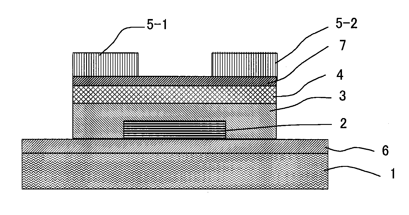
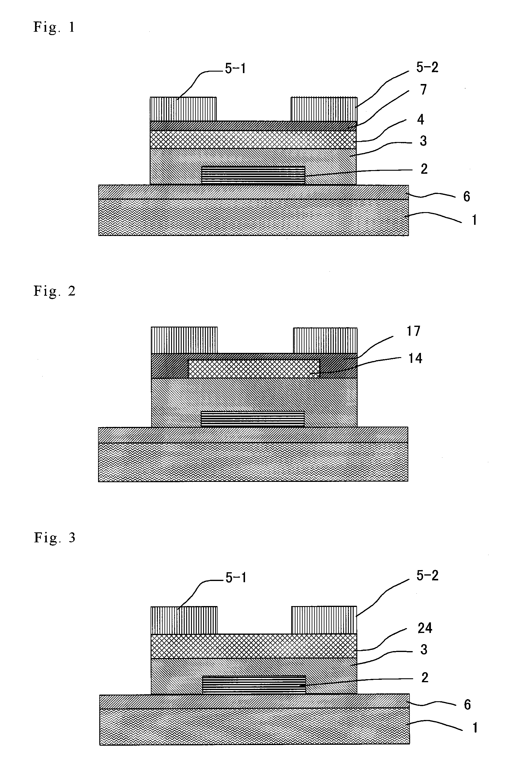
[0296]A substrate and a gate electrode were prepared as follows.
[0297]An N-type Si substrate having a thickness of 0.5 mm (manufactured by Jemco Co., Ltd., electric resistance: from 1 Ωcm to 3.5 Ωcm) was used as a conductive N-type substrate, and this is used as both the substrate and the gate electrode.
[0298]
[0299]Next, on the gate electrode, the following gate insulating layer was formed.
[0300]Gate insulating layer: a gate insulating layer was provided by performing RF magnetron sputtering vacuum deposition of SiO2 (conditions: target of SiO2, temperature for film formation of 54° C., flow rates of sputtering gas Ar / O2=12 sccm / 2 sccm, RF power of 400 W, and film-forming pressure of 0.4 Pa) to form a layer having a thickness of 100 nm. Patterning of the SiO2 gate insulating layer was performed using a shadow mask during sputtering.
[0301]
[0302]Active layer 1: on the gate insulating layer, RF magnetron sputteri...
example 2
[0328]TFT elements were prepared in a similar manner to that in Example 1, except that a barrier-attached film having the following insulating layer, which has a function of barrier, on both sides of a polyethylene naphthalate film (having a thickness of 100 μm) was used instead of the n-Si substrate in Example 1.
[0329]Insulating layer: SiON was deposited to give a thickness of 500 nm. For the deposition of SiON, an RF magnetron sputtering deposition method (conditions for sputtering: target of Si3N4, RF power of 400 W, flow rates of gas Ar / O2=12 sccm / 3 sccm, and film-forming pressure of 0.45 Pa) was applied.
[0330]The obtained elements were evaluated in a similar manner to that in Example 1. As a result, the inventive elements exhibited a small shift quantity of threshold voltage, similar to the results in Example 1.
example 3
1. Preparation of Organic EL Display
[0331](Preparation of Organic EL Element Part)
[0332]1) Formation of Lower Electrode
[0333]As a substrate, the above barrier-attached film including an insulating layer having a function of barrier on both sides of a polyethylene naphthalate film was used. On the substrate, indium-tin oxide (which is referred to hereinafter as ITO) was deposited at a thickness of 150 nm to form an anode.
[0334]2) Formation of Organic Layer
[0335]After cleaning, a hole injection layer, a hole transport layer, a light-emitting layer, a hole blocking layer, an electron transport layer and an electron injection layer were disposed in this order.
[0336]The composition of each layer is as follows. Each layer was provided by resistance heating vacuum deposition.
[0337]Hole injection layer: a layer containing 4,4′,4″-tris(2-naphthylphenylamino)triphenylamine (which is referred to as 2-TNATA) and 2,3,5,6-tetrafluoro-7,7,8,8-tetracyanoquinodimethane (which is referred to as F4-TC...
PUM
 Abstract
Description
Claims
Application Information