Semiconductor wafer, method of producing semiconductor wafer, and heterojunction bipolar transistor

Active Publication Date: 2016-12-22
SUMITOMO CHEM CO LTD
View PDF1 Cites 0 Cited by
  • Summary
  • Abstract
  • Description
  • Claims
  • Application Information

AI Technical Summary

Benefits of technology

The present invention provides a semiconductor wafer with a unique structure that includes different semiconductor layers with specific conductivity types and band gaps. The first semiconductor layer is a p-type or n-type layer, the second semiconductor layer is a different conductivity type, the third semiconductor layer is a p-type layer with a larger band gap, and the fourth semiconductor layer is a p-type layer with a smaller band gap. The fourth semiconductor layer contains a first element that generates a first carrier and a second element that generates a second carrier. The growth of the fourth semiconductor layer is controlled to have a carrier concentration of 1×1019 cm−3 or higher and a mobility of 1000 cm2 / Vs or higher. The semiconductor wafer can be used to produce a heterojunction bipolar transistor with improved performance.

Problems solved by technology

On the other hand, the dopant materials of disilane and monosilane are highly efficiently implanted within a temperature range of 600° C. to 800° C., which is suitable for the vapor-deposition of GaAs crystal layers and AlGaAs layers, but significantly poorly implanted within the temperature range that is suitable for the vapor-deposition of InGaAs crystal layers.”
When the source gas is fed at such a high concentration, however, the dopant materials themselves and silicon resulting from thermal decomposition of the dopant materials contaminate the growth chamber.
Thus, it is difficult to grow highly pure crystal.
When Group-VI atoms such as selenium are used as the n-type dopant for InGaAs, however, the Group-VI atoms such as selenium remain within the epitaxial growth chamber and may unfavorably contaminate a next semiconductor wafer while it is being manufactured.
The atoms such as selenium may diffuse into the underlying layers during the epitaxial growth and compromise the reliability of the devices to be manufactured with the layers.
When silicon atoms are used as the dopant, however, sufficient electrical conductivity cannot be achieved unless a large amount of silicon atoms are implanted as disclosed in Japanese Patent Application Publication No. 7-22327.

Method used


Image

  • Semiconductor wafer, method of producing semiconductor wafer, and heterojunction bipolar transistor
  • Semiconductor wafer, method of producing semiconductor wafer, and heterojunction bipolar transistor
  • Semiconductor wafer, method of producing semiconductor wafer, and heterojunction bipolar transistor

Examples


working example

[0049](Working Example)

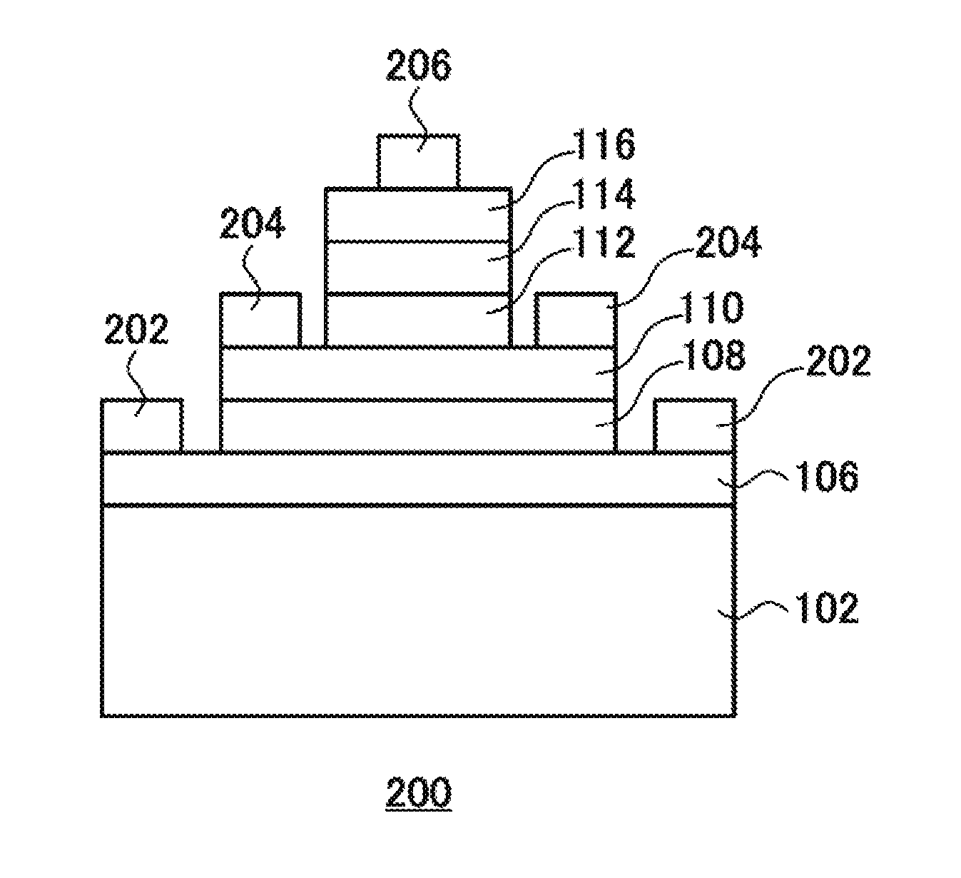
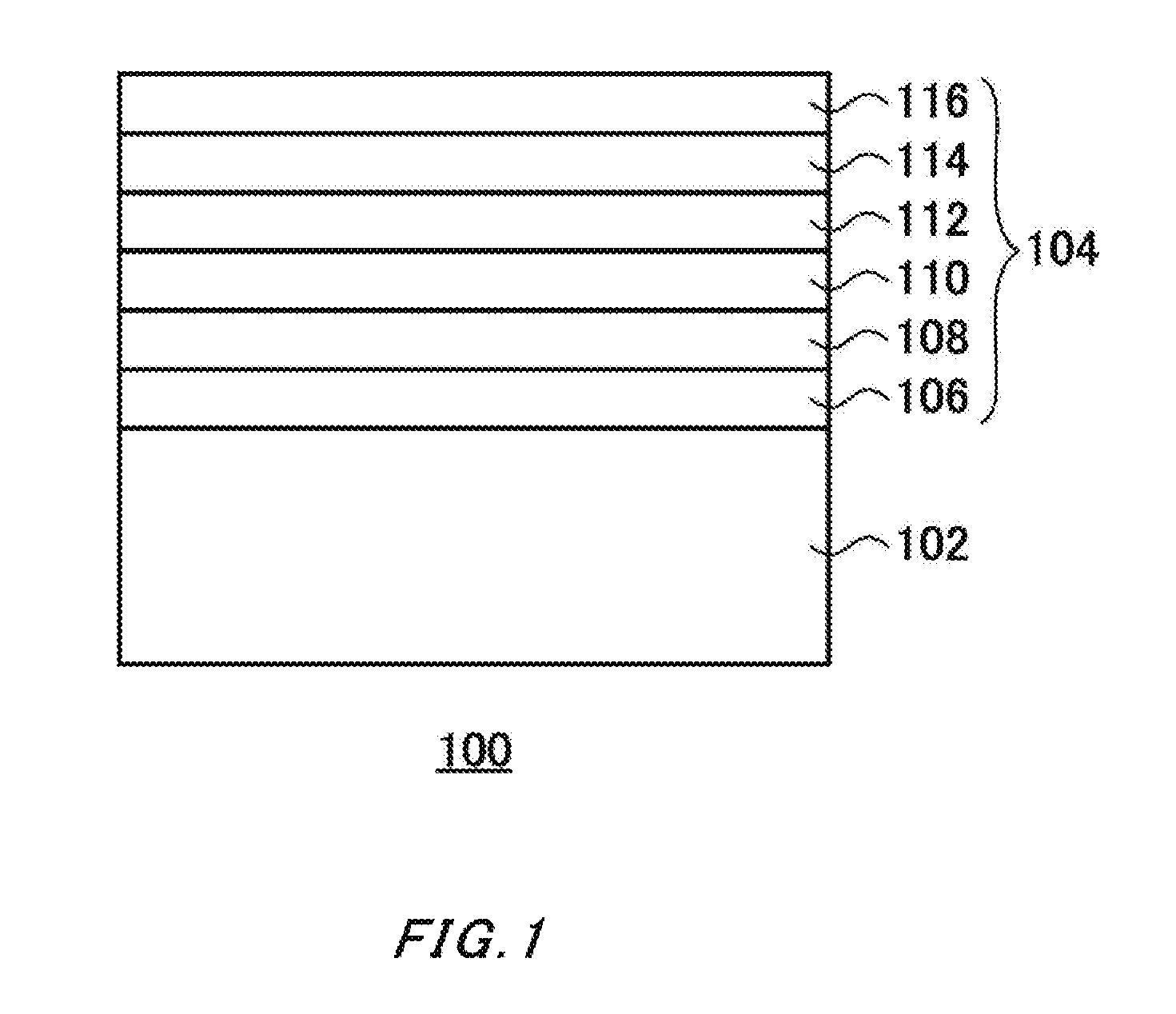
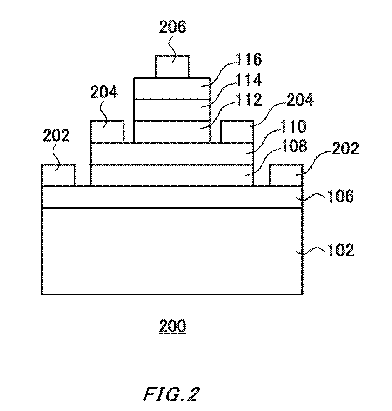
[0050]A semiconductor wafer of a working example was manufactured by sequentially stacking, on a semi-insulative GaAs wafer (the support wafer 102), an n+-type GaAs layer to serve as the sub-collector (the first connection layer 106), an n-type GaAs layer to serve as the collector (the first semiconductor crystal layer 108), a p-type GaAs layer to serve as the base (the second semiconductor crystal layer 110), an n-type InGaP layer to serve as the emitter (the third semiconductor crystal layer 112), an n-type GaAs layer to serve as the sub-emitter (the second connection layer 114) and an n-type InGaAs layer to serve as the emitter contact (the fourth semiconductor crystal layer 116). The n-type InGaP layer to serve as the emitter (the third semiconductor crystal layer 112) had a larger band gap than the p-type GaAs layer to serve as the base (the second semiconductor crystal layer 110). The n-type InGaAs layer to serve as the emitter contact (the fourth semico...


PUM


Abstract

Techniques are provided that can impart sufficient electrical conductivity to a semiconductor crystal exhibiting low doping efficiency for silicon atoms, such as InGaAs, by implanting only a small amount of silicon atoms. Such a semiconductor wafer may include a first semiconductor crystal layer, a second semiconductor crystal layer exhibiting a conductivity type that is different from the first layer, a third semiconductor crystal layer exhibiting the conductivity type of the first layer and having a larger band gap than the second semiconductor crystal layer, and a fourth semiconductor crystal layer exhibiting the conductivity type of the first layer and having a smaller band gap than the third semiconductor crystal layer. The fourth semiconductor crystal layer contains a first element that generates a first carrier of a corresponding conductivity type and a second element that generates a second carrier of a corresponding conductivity type.

Description

BACKGROUND[0001]1. Technical Field[0002]The present invention relates to a semiconductor wafer, a method of producing a semiconductor wafer and a heterojunction bipolar transistor.[0003]2. Related Art[0004]Group III-V compound semiconductor devices such as heterojunction bipolar transistors may have a connection region made of a semiconductor between the semiconductor region providing the operable region and the metal electrode to electrically connect them together. Such a semiconductor connection region preferably forms an ohmic contact with the metal electrode and has low contact resistance. In addition, the connection region itself preferably has low electrical resistance. For this reason, the semiconductor used to form the connection region is often a narrow band-gap semiconductor doped with a large amount of impurity atoms.[0005]For example, when a heterojunction bipolar transistor has a collector made of n-type GaAs, a base made of p-type GaAs, an emitter made of n-type InGaP,...

Claims


Application Information

Patent Timeline
IPC IPC(8): H01L29/66H01L21/02H01L29/207H01L29/737
CPCH01L29/66318H01L29/7371H01L29/207H01L21/02546H01L21/0262H01L21/02395H01L21/02461H01L21/02463H01L21/02505H01L21/02576
Inventor YAMANAKA, SADANORINISHIKAWA, NAOHIRONAKANO, TSUYOSHI
Owner SUMITOMO CHEM CO LTD
Why Eureka
Try Eureka