E-field-modulated bistable molecular mechanical device
- Summary
- Abstract
- Description
- Claims
- Application Information
AI Technical Summary
Benefits of technology
Problems solved by technology
Method used
Image
Examples
second embodiment
[0076] Since each colorant molecule in colorant layer 301 is transparent outside of the colorant absorption band, then multiple colorant layers may be superimposed and separately addressed to produce higher resolution color displays than currently available. FIG. 4 is a schematic illustration of this A high resolution, full color, matrix addressable, display screen 400 comprises alternating layers of transparent electrodes--row electrodes 401, 403 and column electrodes 402 and 404- and a plurality of colorant layers 405, 407, 409, each having a different color molecule array. Since each pixel in each colorant layer may be colored or transparent, the color of a given pixel may be made from any one or a combination of the color layers (e.g., cyan, magenta, yellow, black) at the full address resolution of the display. When all colorant layers 405, 407, 409 for a pixel are made transparent, then the pixel shows the background substrate 303 (e.g., white). Such a display offers the benef...
third embodiment
[0079] More specifically, the third embodiment as shown in FIG. 5 comprises a display screen 502, a scanned electrode array 504, and array translation mechanism 501 to accurately move the electrode array across the surface of the screen. The display screen 502 again comprises a background substrate 303, a transparent view-through layer 305, and at least one bi-stable molecule colorant layer 301. The colorant layer 301 may include a homogeneous monochrome colorant (e.g., black) or color mosaic, as described herein above. The scanned electrode array 504 comprises a linear array or equivalent staggered array of electrodes in contact or near contact with the background substrate 303. A staggered array of electrodes may be used, for example, to minimize field crosstalk between otherwise adjacent electrodes and to increase display resolution.
[0080] In operation, each electrode is sized, positioned, and electrically addressed to provide an appropriate electric field, represented by the arr...
example 1b
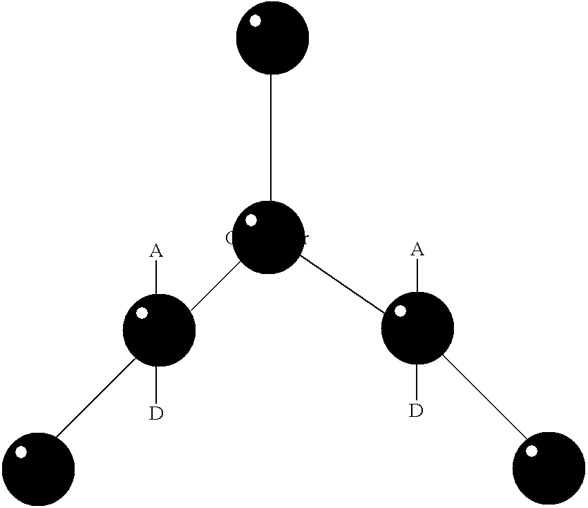
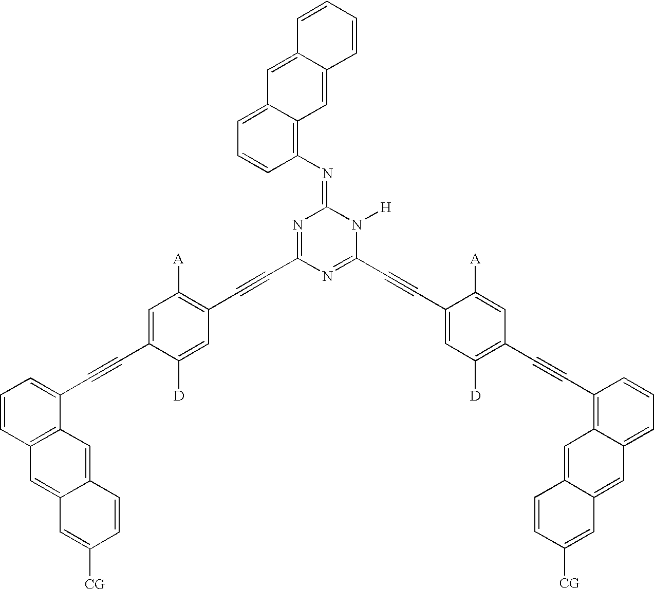
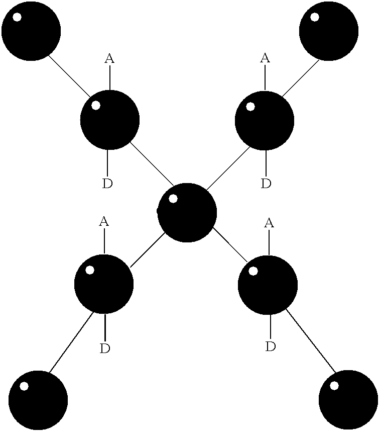
[0112] Example 1b below is a real molecular example of this embodiment. 2
[0113] where:
[0114] A is the Acceptor group;
[0115] D is the Donor group; and
[0116] CG are optional connecting units between one molecule and another molecule or between a molecule and the solid substrate. They can be a single connecting unit or multiple connecting units. They may be any one of the following: hydrogen (utilizing a hydrogen bond), multivalent hetero atoms (i.e., C, N, O, S, P, etc.), functional groups containing these hetero atoms (e.g., NH, PH, etc.), hydrocarbons (either saturated or unsaturated), or substituted hydrocarbons.
[0117] In Example 1b above, the horizontal dashed lines represent other molecules or solid substrates (which can be either electrode or non-electrode depends on applications) to which the molecule is optionally linked. The direction of the switching field is perpendicular to the horizontal dotted lines. Alternatively, the linking moieties (CG) may be eliminated, and the mol...
PUM
| Property | Measurement | Unit |
|---|---|---|
| Angle | aaaaa | aaaaa |
| Band gap | aaaaa | aaaaa |
| Transparency | aaaaa | aaaaa |
Abstract
Description
Claims
Application Information


