Capacitor and semiconductor device including dielectric and N-type semiconductor

a semiconductor and capacitor technology, applied in capacitors, solid-state devices, transistors, etc., can solve the problems of large amount of tunnel current due to quantum effects, large energy difference, and large energy difference between high-k materials, and achieve stable chemically stable and favorable adhesion with high-k materials

Active Publication Date: 2013-08-20
SEMICON ENERGY LAB CO LTD
View PDF142 Cites 5 Cited by
  • Summary
  • Abstract
  • Description
  • Claims
  • Application Information

AI Technical Summary

Benefits of technology

[0021]It is an object of one embodiment of the prevent invention to provide a capacitor using a high-k material, at a low cost. Further, it is another of one embodiment of the prevent invention to provide a capacitor using a high-k material that is formed over a surface having a peculiar shape with good coverage. Furthermore, it is another of one embodiment of the prevent invention to provide a capacitor suitable for highly miniaturization.
[0027]Indium oxide, zinc oxide, and the like are known as oxide semiconductors having a band gap of 2.5 eV or higher, and a material having an electron affinity of 4.6 eV or lower of such oxide semiconductors has a potential barrier of 1 eV or higher with an n-type semiconductor in one embodiment of the present invention. Since such a material has a large band gap, it has few thermally excited carriers to be intrinsic and thus has high resistance.
[0048]Most of high-k materials are oxides, and thus when oxygen is contained in the elements other than a metal element, among the elements constituting a high-work-function compound semiconductor, at 20 at. % to 90 at. %, the adhesiveness with the high-k material is favorable. In addition, an oxidation-reduction reaction hardly occurs at the interface, and thus the interface is stable chemically.

Problems solved by technology

A problem in the use of such a high-k material is generally that the electron affinity (the energy difference between a vacuum level and a bottom of a conduction band) of such a high-k material is large.
Even with the potential barrier of about 1.5 eV, if the thickness of a dielectric is 5 nm or more, a noticeable problem does not occur in an insulating property, but when the thickness of a dielectric is desirably 3 nm or less along with miniaturization of a circuit, the amount of a tunnel current due to a quantum effect becomes large, so that sufficient function as a capacitor is not met, which is a problem.
In addition, tantalum oxide, barium strontium titanate, lead titanate, lead zirconate, barium zirconate, or the like having a higher permittivity has a potential barrier of 0.5 eV or lower in a junction with n-type silicon, and thus a sufficient insulating property is difficult to be obtained even when the thickness of a dielectric is 10 nm or more.
On the contrary, when the potential barrier is less than 1 eV, the dielectric is not suitable for a capacitor.
However, such metals having a high work function are expensive, and there is no other practical method for forming a thin film of such a metal, except a physical formation method such as a sputtering method.
By a physical formation method, for example, it is difficult to form a film with a good coverage, over an object having a peculiar shape such as a trench-type capacitor or a stack-type capacitor used in DRAM or the like.

Method used


Image

  • Capacitor and semiconductor device including dielectric and N-type semiconductor
  • Capacitor and semiconductor device including dielectric and N-type semiconductor
  • Capacitor and semiconductor device including dielectric and N-type semiconductor

Examples


embodiment 1

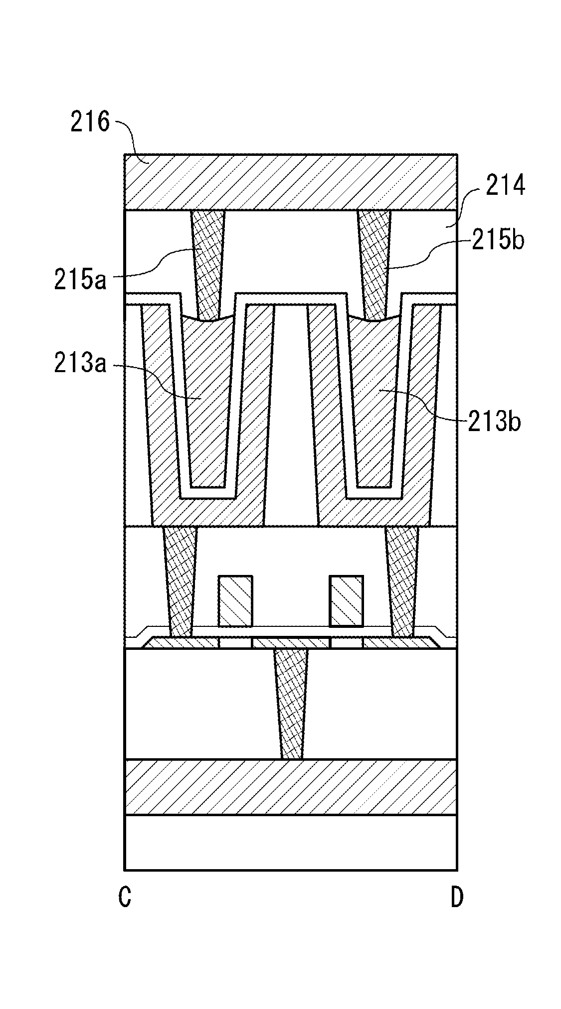
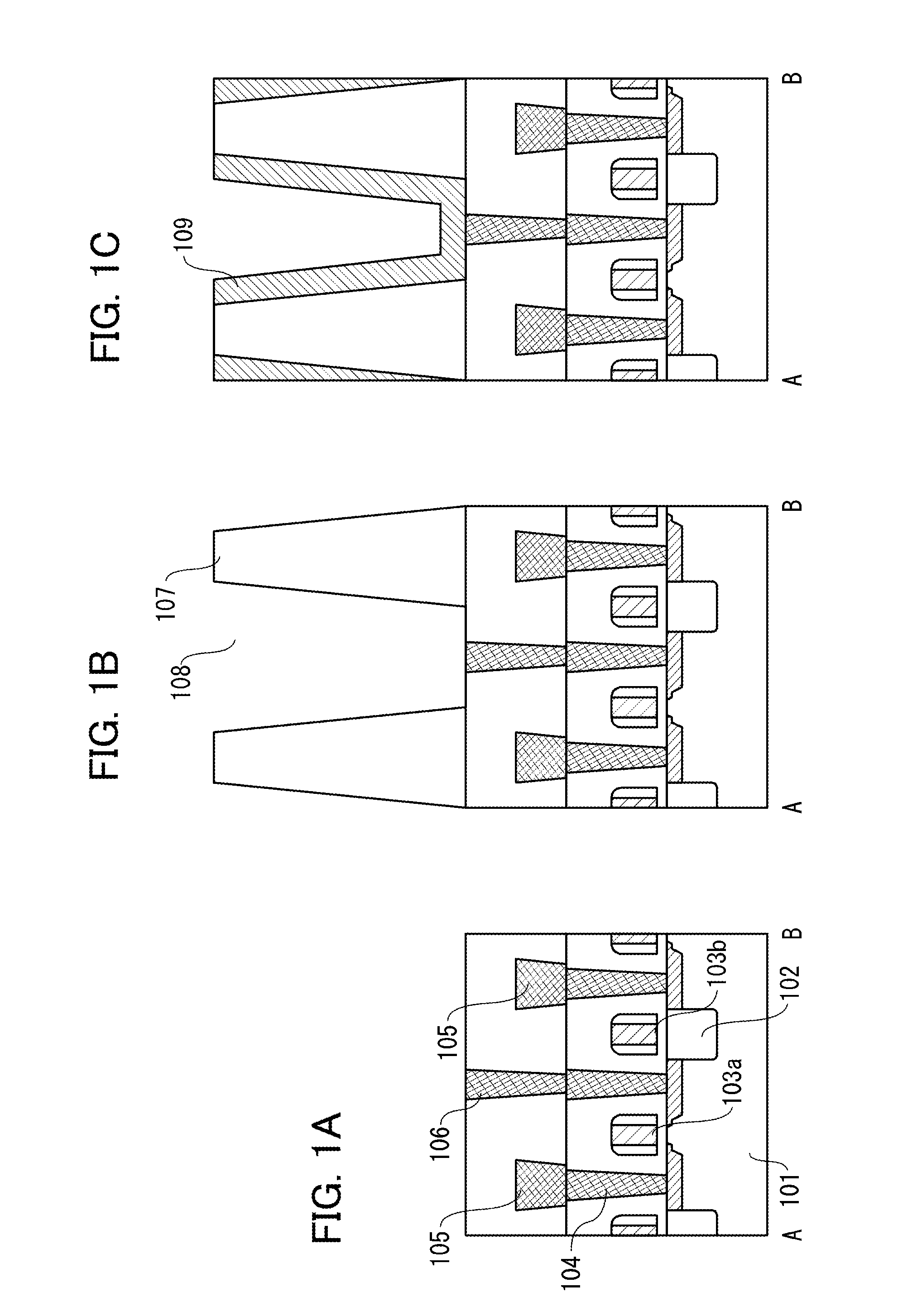
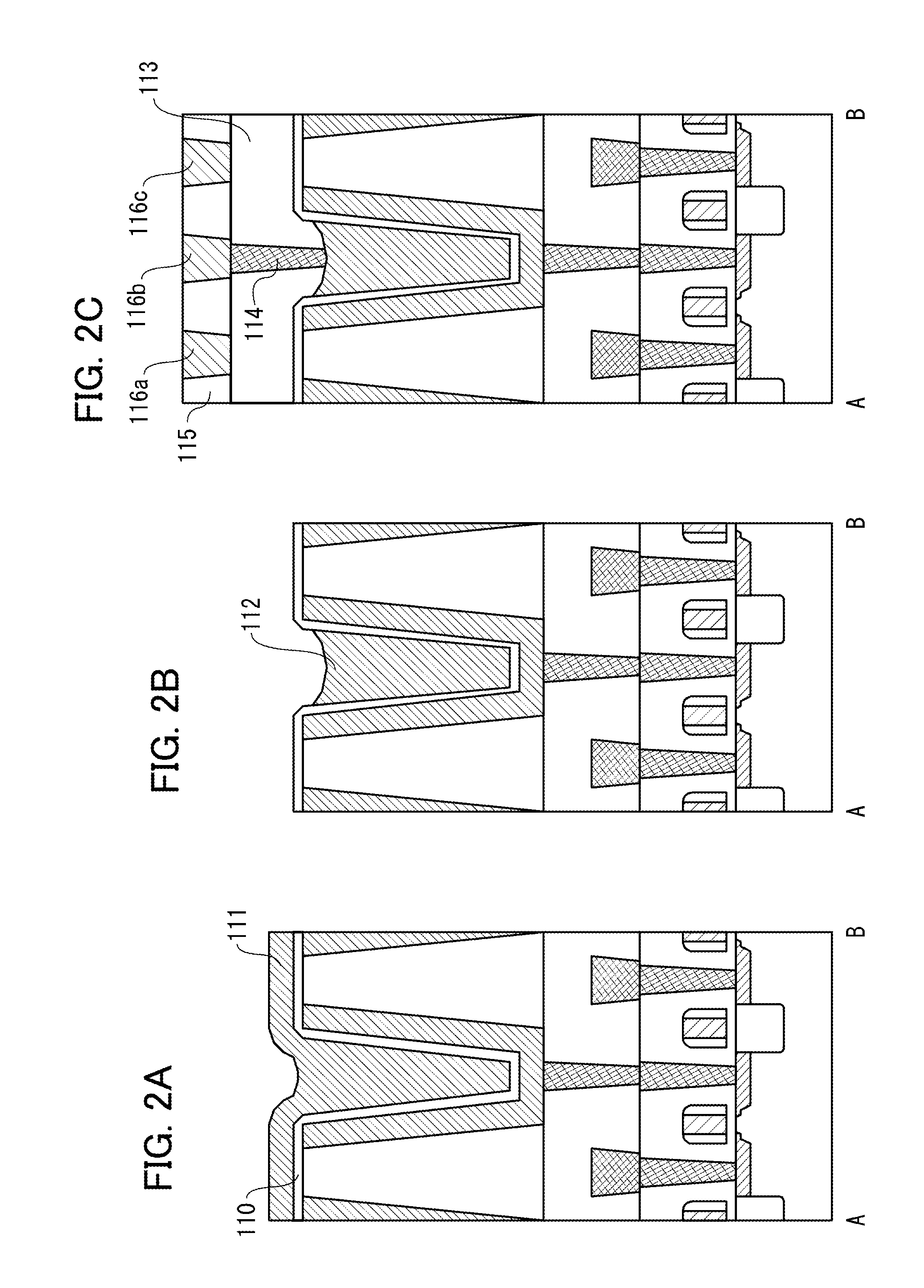
[0059]In FIG. 1A to FIG. 1C, FIG. 2A to FIG. 2C, and FIG. 4A to FIG. 4D, an example of a manufacturing process of a semiconductor device (a DRAM having a stack-type capacitor) in this embodiment is illustrated. Note that unless otherwise specified, for materials used, methods, and the like, those of known manufacturing techniques of semiconductor integrated circuits may be referred to.

[0060]FIG. 1A to FIG. 1C and FIG. 2A to FIG. 2C are cross-sectional views of a manufacturing process of a semiconductor device in this embodiment, and FIG. 4A to FIG. 4D are schematic top views of the manufacturing process of the semiconductor device in this embodiment. In FIG. 4A to FIG. 4D, only major wirings and the like are illustrated. The cross-sections taken along the dashed-dotted line A-B in FIG. 4A to FIG. 4D correspond to the cross-sectional views of FIG. 1A to FIG. 1C and FIG. 2A to FIG. 2C.

[0061]In this embodiment, manufacturing of a so-called folded-bit-line DRAM is described. In such a f...

embodiment 2

[0078]This embodiment is illustrated in FIG. 3A to FIG. 3C and FIG. 4E and FIG. 4F. In this embodiment, an open-bit-line DRAM is manufactured using a thin film transistor. The area of a memory cell of an open-bit-line DRAM can be downsized to 6 F2 (F is a feature size) ideally, which is smaller than that of the folded-bit-line DRAM described in Embodiment 1. Hereinafter, description is given with reference to the drawings.

[FIG. 3A]

[0079]A bit line 202 is formed over a first insulator 201. Further, a second insulator 203 is formed, and a first contact plug 204 connected to the bit line 202 is formed in the second insulator 203. Further, a semiconductor layer 205 with an appropriate thickness and size, a third insulator 206 covering the semiconductor layer 205, and word lines 207a and 207b are formed. The third insulator 206 serves also as a gate insulating film of a thin film transistor.

[0080]There are no particular limitations on the semiconductor layer 205, and single crystal, poly...

embodiment 3

[0088]This embodiment is illustrated in FIGS. 5A to 5E and FIGS. 6A and 6B. In this embodiment, a signal-amplification type memory cell (see Reference 4) using two transistors is formed.

[0089]FIG. 6A is a circuit diagram of a memory cell of a normal DRAM having one transistor and one capacitor (also referred to as 1T1C DRAM) described in Embodiment 1 or Embodiment 2. In the DRAM, a writing transistor WT is turned on or off in response to a potential of a word line WL, and a charge is transferred between the bit line BL and a capacitor CS. Thus, in accordance with a parasitic capacitance of the bit line BL, the capacitance of the capacitor CS should be determined, and even if the design rule is smaller, a nearly equal capacitance is needed. For that reason, it is necessary to employ a trench-type capacitor or a stack-type capacitor, or further a high-k material.

[0090]On the contrary, a memory cell illustrated in FIG. 6B has two transistors and one capacitor. Charges stored in the cel...


PUM

PropertyMeasurementUnit
work functionaaaaaaaaaa
thicknessaaaaaaaaaa

Abstract

A capacitor that has an electrode of an n-type semiconductor that is provided in contact with one surface of a dielectric, has a work function of 5.0 eV or higher, preferably 5.5 eV or higher, and includes nitrogen and at least one of indium, tin, and zinc. Since the electrode has a high work function, the dielectric can have a high potential barrier, and thus even when the dielectric is as thin as 10 nm or less, a sufficient insulating property can be maintained. In particular, a striking effect can be obtained when the dielectric is formed of a high-k material.

Description

BACKGROUND OF THE INVENTION[0001]1. Field of the Invention[0002]The present invention relates to capacitors used for semiconductor devices and semiconductor devices using the capacitors.[0003]2. Description of the Related Art[0004]Capacitors used for semiconductor integrated circuits and the like have conventional structures in each of which a dielectric such as silicon oxide is sandwiched between electrodes made of a metal or a semiconductor such as silicon with high conductivity. However, as circuits are miniaturized, the use of materials having higher permittivity (high-k materials) than silicon oxide (relative permittivity around 4) has begun to be studied.[0005]A problem in the use of such a high-k material is generally that the electron affinity (the energy difference between a vacuum level and a bottom of a conduction band) of such a high-k material is large. For example, according to Reference 6, the electron affinity of silicon oxide is 0.9 eV, while the electron affinity o...

Claims


Application Information

Patent Timeline
Patent Type & Authority Patents(United States)
IPC IPC(8): H01L29/00H01L29/94H01L29/76H01L27/108H01L31/119H01L31/113H01L31/062
CPCH01L21/84H01L27/10852H01L27/10885H01L27/11551H01L27/1156H01L27/1203H01L27/1207H01L28/91H01L27/0207H01L27/10873H10B12/05H10B12/033H10B12/482H10B41/70H10B41/20H10B99/00H10B12/00
Inventor TAKEMURA, YASUHIKO
Owner SEMICON ENERGY LAB CO LTD
Why Eureka
Try Eureka